 Part of the Oxford Instruments Group
Expand
Collapse
Part of the Oxford Instruments Group
We had the privilege to speak with two Senior Research Fellows from UCL who use our PlasmaPro® 80 RIE system, presenting their latest research projects related to Quantum and Optoelectronic devices.
Dr Oscar Kennedy has used the PlasmaPro 80 RIE system to create a superconducting circuit by etching the superconducting NbN film, whereas Dr Wing Ng has used the RIE system to accurately pattern a 50 nm gap with smooth sidewalls between a pair of waveguides for chip‑based optical buffers.
Reactive Ion Etching offers excellent process control in the fabrication of semiconductor devices and is used in many device manufacturing processes.
Download Case StudyDr Oscar Kennedy, UCLQ Postdoctoral Fellow, focuses on the fabrication of devices for the efficient exchange of quantum information. The main goal of his research is to create Quantum Memories which are essential to overcome decoherence limitations and scale quantum information systems for more sophisticated computations.
Superconducting resonators are fabricated on silicon using standard photolithography techniques with Nb or NbN as the superconducting metal. The resonators are designed and fabricated to have a resonant frequency that can be tuned by a magnetic field component introduced in an orientation perpendicular to the thin film resonator. This tunability enables optimal coupling between the superconducting resonator and the spin system.
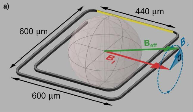
Schematic of the lumped element NbN thin-film resonator and the applied magnetic field Beff with two components (Source: https://aip.scitation.org/doi/full/10.1063/1.5129032)
In previous research, Dr Kennedy used lift-off techniques for the fabrication of the superconducting architecture. However, as he states “some of the better results for quantum devices have been achieved by etching rather than lift-off techniques". Oxford’s PlasmaPro RIE system is used to create the superconducting circuit by etching the superconducting NbN film.

"With the PlasmaPro RIE, you can proceed with very aggressive chemical cleaning and then immediately deposit your superconductor on top of your substrate. It’s fast to use and straightforward with powerful and immediate results."
Dr Oscar Kennedy, UCLQ Postdoctoral Fellow
Etch processes are superior for many quantum device fabrication applications because there is no need to apply photoresist to the bare Silicon surface, thus avoiding lossy organic residues at the metal-substrate interface. These residues cannot be removed in a lift-off process because some photoresist must be present on the wafer at the time of metal deposition in a lift-off process, which makes it impossible to use aggressive cleaning techniques to remove organic residue at a similar surface where the superconductor will remain after deposition.
Read the full Case StudyDr Wing Ng, Senior Research Fellow in nanofabrication and optoelectronics at UCL, has focused on optical networks which is the future of data communication.
As the signal in optical fibres travels between multiple destinations and devices, the light needs to switch the data to separate destinations. If two or more signals arrive at the optical switch at the same time, one or more of the signals must wait while the first signal is switched. The current technology is slow and not energy efficient, as the signal needs to be converted into an electrical domain before storing it in an electronic memory.
Dr Ng’s research is dedicated to finding a way to store this information in the optical domain using an optical buffer, a device that provides optical delay (memory) for optical switching systems. This technology is more energy-efficient, as it would eliminate the need for electrical-optical signal conversion.
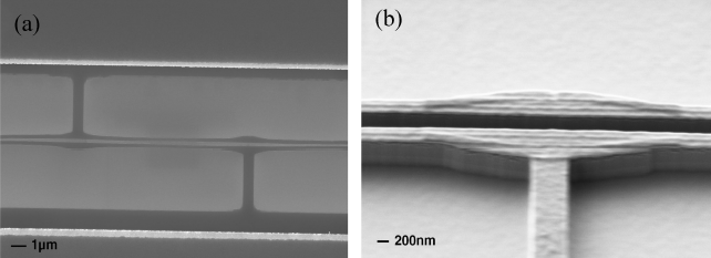
SEM images of (a) top view of the waveguide and pillar pattern after electron beam lithography, (b) side view of the reactive ion etched pillar section of the structure. (Source: https://ieeexplore.ieee.org/document/6994243)
Dr Ng and his colleagues designed a chip-based optical buffer, and the heart of the system is a pair of suspended parallel waveguides fabricated out of indium phosphide material (InP).
“The optical delay time for our system depends on the separation distance between the two parallel waveguides, as well as the overall length of the waveguides”, says Dr Ng. This has been achieved with reactive ion etching after the patterning of the waveguides with electron beam lithography.

“Oxford’s RIE system offers high flexibility in the process and excellent control of the gases and the power of plasma”.
Dr Wing Ng, Senior Research Fellow at UCL
The PlasmaPro 80 RIE system enabled Dr Ng to accurately pattern the 50 nm gap between the pair of waveguides with smooth sidewalls and a sidewall angle above 80°, without leaving any residual resist on the waveguide surfaces.
Our reactive ion etching system achieves smooth waveguide sidewalls, which is important to minimize light leakage and propagation losses in optoelectronic devices.
Read the full Case Study
© Oxford Instruments 2026

