 Part of the Oxford Instruments Group
Expand
Collapse
Part of the Oxford Instruments Group


At the Advanced Semiconductor Laboratory (ASL) at King Abdullah University of Science and Technology (KAUST), our research group, led by Professor Xiaohang Li, uses an Oxford Instruments PlasmaPro 100 Atomic Layer Etch (ALE) system to explore how atomic-scale surface processing can improve next-generation semiconductor devices. We explore many applications of III-V semiconductors, such as Light-Emitting Diodes (LEDs)1,2, Schottky Barrier Diodes (SBDs)3 and Metal-Oxide-Semiconductor Field-Effect Transistors (MOSFETs)4 (Figure 1). One limitation to further enhancing these devices is etch-induced surface and interface damage, as is widely reported in the literature5-10. It is therefore important to investigate practical ways to remove or avoid this damage while remaining compatible with current fabrication flows.
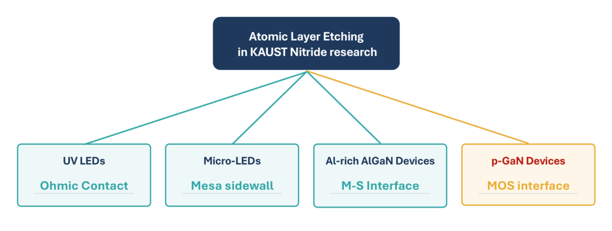
Figure 1: KAUST has applied ALE as a low-damage interface-engineering step across electronic and optoelectronic technologies.
One such avenue under investigation is ALE, a process of sequential, self-limiting half-cycles that enables material to be removed at the nm-scale and below. The basic idea for an ALE cycle can be seen in Figure 2. In each cycle, the exposed semiconductor surface is first chemically modified e.g. by chlorination, followed by a purge step to remove residual reactants. A low-power Ar plasma is then used to selectively remove the modified surface layer, after which a second purge completes the cycle. By ensuring that the removal step is highly selective to the modified layer, the underlying material is minimally affected, and therefore minimal damage occurs. However, because of its cyclic nature, ALE typically has a lower etch rate than conventional approaches such as inductively coupled plasma reactive ion etching (ICP-RIE). This makes ALE less suitable for rapid removal of relatively thick material layers, but particularly attractive for the controlled finishing of surfaces and interfaces where minimizing etch-induced damage is critical.
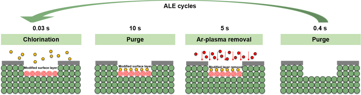
Figure 2: Schematic of a typical ALE cycle showing sequential surface chlorination, purge, Ar-plasma removal, and final purge steps.
With access to KAUST’s shared research facilities and technical support from Dr. Syed Kazmi at KAUST Core Labs, our team has applied ALE to a wide range of electronic and optoelectronic technologies. Our work demonstrates that ALE is much more than a precise (but slow) etching technique. Rather than replacing conventional plasma etching entirely, ALE can be used strategically as a low-damage finishing step after rapid material removal. When used in this way, it can remove damaged surface layers, improve critical interfaces, and deliver substantial gains in device performance and device-to-device uniformity.
In this blog post, we take a closer look at how ALE is helping enable p-channel GaN MOSFETs for future GaN CMOS integration, through research led by Zixian Jiang, a PhD researcher at KAUST.
To achieve enhancement-mode operation in GaN pFETs, p-GaN gate recessing using ICP-RIE has become a widely adopted strategy. In such devices, most of the p-GaN beneath the gate must be recessed while retaining a thin 14 nm channel layer. This requirement creates a challenging process window: the etch must be sufficiently deep and precisely controlled, while the remaining p-GaN layer forms the foundation for the gate dielectric and channel interface. In addition, the etched p-GaN surface can create a high density of trap states at the oxide/p-GaN interface. These traps severely degrade the subthreshold characteristics and induce substantial device-to-device variation, resulting in increased off-state leakage and reduced on-current.
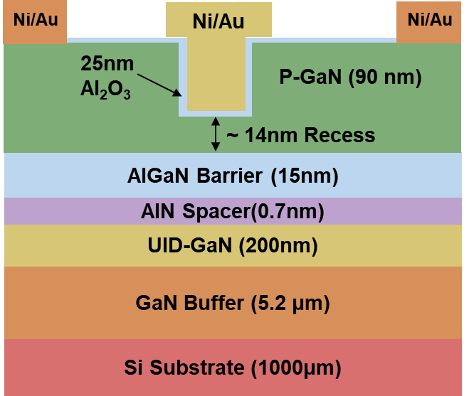
Figure 3: Schematic cross-section of the enhancement-mode GaN p-FET (LGS/LG/LGD = 5/3/15 µm).
In this context, ALE provides precise thickness control, minimal surface damage, improved surface morphology, and enhanced device-performance uniformity. However, its low etch rate makes it impractical for removing the entire thick p-GaN layer.
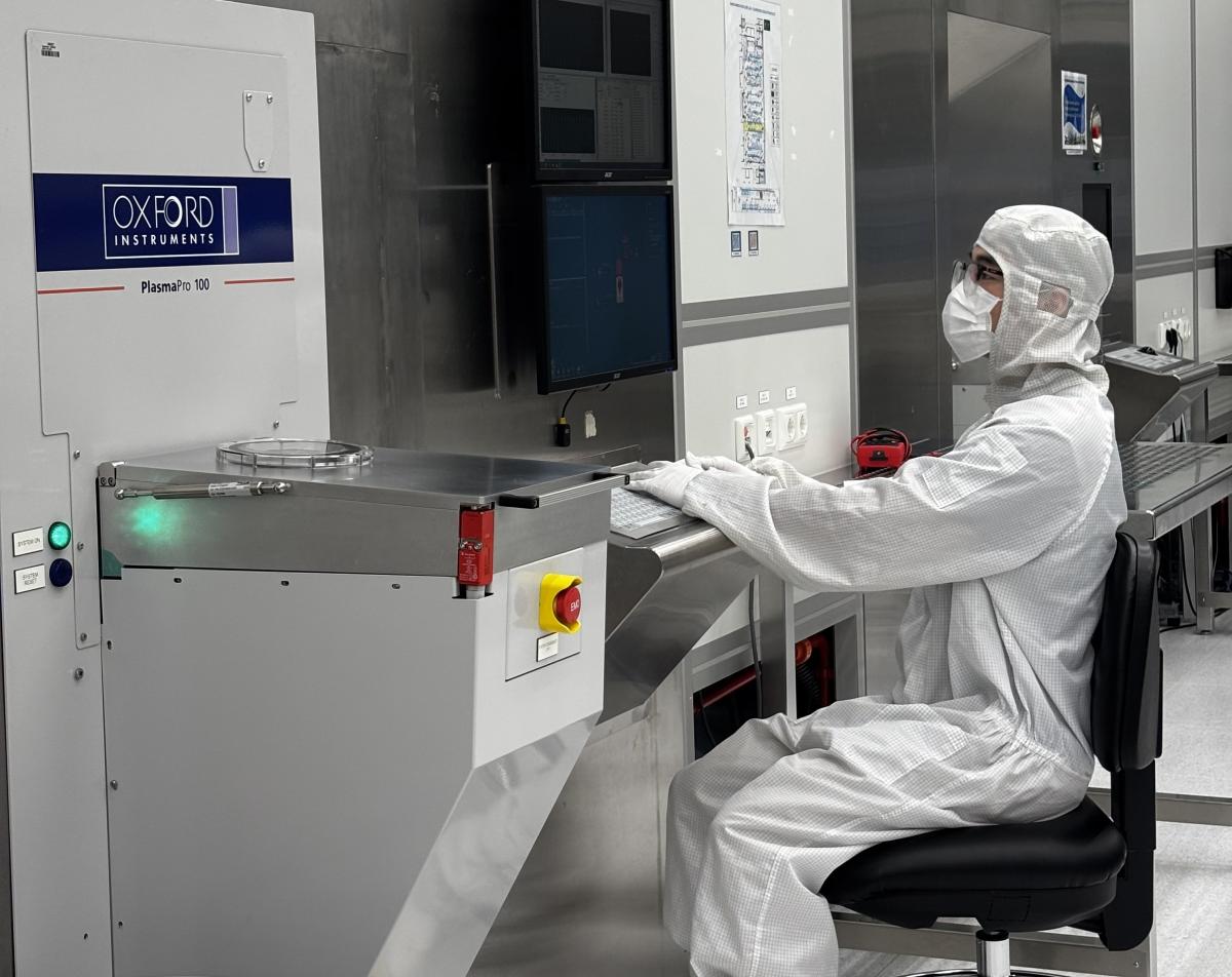
Figure 4: Oxford Instruments PlasmaPro platform at KAUST.
One approach to achieving the desired recess step while maintaining throughput is a sequential process that combines the speed of ICP-RIE with the atomic-scale control of ALE. To investigate sequential processing, we compared two otherwise matched process flows. In the reference devices, approximately 76 nm of p-GaN was removed entirely by ICP-RIE. In the sequential process, ICP-RIE rapidly removed the first approximately 60 nm, while ALE precisely removed the final approximately 16 nm and refined the recessed surface. Both processes retained approximately 14 nm of GaN above the AlGaN barrier, ensuring that the electrical comparison reflected the effect of the final surface treatment rather than differences in recess depth.
The Oxford Instruments PlasmaPro 100 system provides a key advantage for this sequential approach: ICP-RIE and ALE can be performed sequentially in the same chamber without breaking vacuum. Each ALE cycle consists of chlorine dosing to modify the exposed surface, a purge step, low-power argon-plasma removal, and a purge step.
This sequential ICP-RIE + ALE strategy therefore delivers the best of both processes: rapid material removal for deep recessing, followed by low-damage, atomic-scale finishing of the critical gate interface. This benefit is evident in Figure 5(b) and (c), where the ALE finishing step produces a smoother surface. The next question is how this interface improvement translates within a complete device fabrication flow.
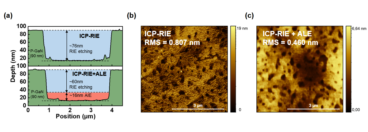
Figure 5: Sequential p-GaN gate recess strategy and ALE cycle. ICP-RIE provides fast material removal; ALE completes the final approximately 16 nm while reducing the damaged surface layer. Atomic force microscopy (AFM) measurements show that RMS roughness decreased from 0.807 nm to 0.460 nm.
By adopting this sequential ICP-RIE+ALE strategy, the fabrication of GaN pFETs sequence began with mesa isolation and the formation of Ni/Au source/drain contacts. A 200 nm SiO₂ hard mask was then used to define the 3 μm gate window. ICP-RIE removed the main approximately 60 nm portion of the p-GaN recess, after which ALE removed the final approximately 16 nm in the same chamber without an intermediate vacuum break. The hard mask and surface residues were subsequently removed, followed by the deposition of a 25 nm Al₂O₃ gate dielectric by PE-ALD on an Oxford Instruments PP-ASP, Ni/Au gate metallization, and opening of the contact windows.
The impact of ALE is clearly visible in cross-sectional TEM images. As shown in Figure 6(a) after conventional ICP-RIE, the recessed p-GaN surface contains a damaged layer, with defects extending into the GaN beneath the Al2O3 gate dielectric. The recess edges in Figure 6(b) are also slightly rounded, which is a sign of uncontrolled material removal and plasma-induced damage.
Adding an ALE finishing step changes this picture dramatically. The p-GaN/Al2O3 interface becomes smoother and more abrupt, with substantially reduced interfacial damage, as illustrated in Figure 6(c). The recess corners, Figure 6(d), also remain much sharper, highlighting the superior profile control provided by ALE’s layer-by-layer removal mechanism. In effect, ALE gently removes the damaged surface, smooths the recess, and improves the sidewall profile before the critical gate dielectric is deposited.
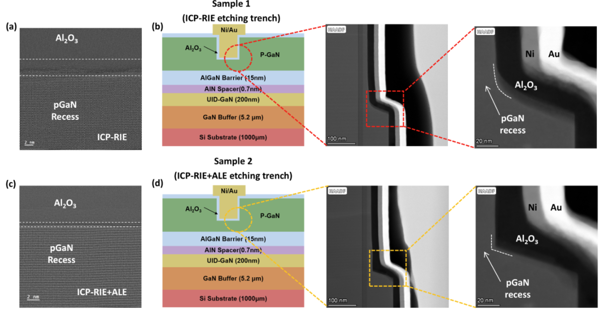
Figure 6: Cross-sectional TEM/HAADF comparison of the recessed gate region and Al2O3/p-GaN interface after ICP-RIE and ICP-RIE + ALE processing.
These improvements are not only visible under the microscope, they also translate directly into better device performance (Figure 7). The ICP-RIE + ALE devices delivered improved switching, lower leakage, and, importantly, much greater device-to-device consistency. The mean subthreshold swing decreased from 365 to 149 mV/dec, while its standard deviation fell from 179 to just 17 mV/dec. Off-state leakage was reduced by more than an order of magnitude and became substantially more consistent. The devices also achieved approximately four times higher saturation current and twice the peak transconductance of the ICP-RIE-only reference.4
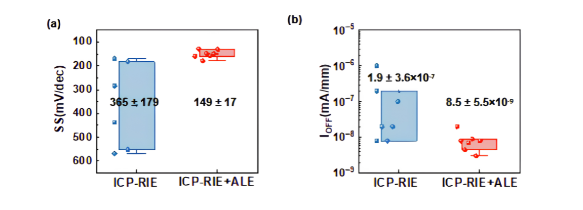
Figure 7: Statistical comparisons of (a) subthreshold swing (SS) and (b) off-state leakage (IOFF), plotted with mean ± standard-deviation error bars.
For practical GaN CMOS integration, this combination of higher performance and tighter uniformity is especially valuable. ALE finishing provides a way to improve not only the best-performing device, but the entire device population, delivering cleaner interfaces, stronger performance, and more consistent results from one device to the next.
The p-channel GaN MOSFET results demonstrate that the value of ALE extends far beyond precise material removal. By removing plasma-damaged surface layers before gate-interface formation, ALE improves the device characteristics that matter most for future integrated technologies: switching control, leakage current, drive current, and device-to-device uniformity.
These benefits are not limited to GaN MOSFETs. Across ASL’s broader research programme, ALE has been applied wherever conventional plasma etching leaves damage near a performance-critical interface. It has proven highly effective across III-V materials such as GaN, AlInN, AlGaN, and AlN, with applications including deep-ultraviolet (DUV) LEDs1, green micro-LEDs2, Al-rich AlGaN SBDs3 and GaN CMOS4. Although these devices serve different functions, the role of ALE remains consistent: precisely preventing damage where it matters most.
Together, these results clearly demonstrate that ALE is more than a slow, highly controlled etching technique. When strategically combined with conventional plasma processing, it becomes a targeted interface-engineering solution that translates atomic-scale surface control into measurable improvements in efficiency, voltage handling, switching performance, and manufacturing uniformity, helping enable the next generation of nitride semiconductor devices.
Learn more about KAUST Advanced Semiconductor Laboratory, KAUST Core Labs and Oxford Instruments atomic layer etching solutions.
Selection of related publications:
To discover whether Oxford Instruments can support and develop your application, please get in touch with our team and we will be happy to discuss how our tools can benefit you.
Ask a question
Follow our publications page to see what our customers and our researchers at Plasma Technology are doing with our systems.
Keep in touch with our Oxford Instruments Semiconductors page on LinkedIn to find out what conferences you can speak to us at and all of our latest updates.
1. Z. Liu, T. Liu, H. Cao, Z. Jiang, N. Xiao, G. I. M. Garcia, . . . X. Li, Opt. Lett. 49, 4533-4536 (2024). https://doi.org/10.1364/OL.530...
2. Z. Liu, H. Cao, T. Liu, Y. Lu, X. Tang, Z. Jiang, . . . X. Li, Opt. Lett. 50, 3756-3759 (2025). https://doi.org/10.1364/OL.561...
3. T. Liu, Z. Liu, H. Cao, M. Nong, X. Tang, Z. Jiang, . . . X. Li, Appl. Phys. Lett. 126, 152109 (2025). https://doi.org/10.1063/5.0251...
4. Z. Jiang, Z. Liu, T. Liu, H. Cao, S. Yuvaraja, G. I. M. García, . . . X. Li, Appl. Phys. Lett. 128, 153504 (2026). https://doi.org/10.1063/5.0319...
5. K.-W. Kim, S.-D. Jung, D.-S. Kim, H.-S. Kang, K.-S. Im, J.-J. Oh, . . . J.-H. Lee, IEEE Electron Device Lett. 32, 1376-1378 (2011). https://doi.org/10.1109/LED.20...
6. C. Yang, H. Fu, P. Peri, K. Fu, T.-H. Yang, J. Zhou, . . . Y. Zhao, IEEE Electron Device Lett. 42, 1128-1131 (2021). https://doi.org/10.1109/led.20...
7. Z. Zheng, W. Song, L. Zhang, S. Yang, J. Wei, and K. J. Chen, IEEE Electron Device Lett. 41, 26-29 (2020). https://doi.org/10.1109/led.20...
8. W. Y. Ho, Y. C. Chow, Z. Biegler, K. S. Qwah, T. Tak, A. Wissel-Garcia, . . . J. S. Speck, Appl. Phys. Lett. 123, 062102 (2023). https://doi.org/10.1063/5.0159...
9. N. Chowdhury, J. Lemettinen, Q. Xie, Y. Zhang, N. S. Rajput, P. Xiang, . . . T. Palacios, IEEE Electron Device Lett. 40, 1036-1039 (2019). https://doi.org/10.1109/led.20...
10. H. Du, Z. Liu, T. Zhang, L. Hao, G. Gao, W. Xing, . . . Y. Hao, in 2023 7th IEEE Electron Devices Technology & Manufacturing Conference (EDTM) (2023), pp. 1-3. https://doi.org/10.1109/edtm55...

Zixian Jiang is a PhD researcher in Electrical and Computer Engineering at KAUST under supervision of Prof. Xiaohang Li. His research focuses on wide-bandgap semiconductors, particularly GaN-based power devices and complementary metal–oxide–semiconductor (CMOS) technology for energy-efficient systems. He has experience in epitaxial growth, semiconductor nanofabrication, atomic layer etching and device characterisation.

Dr. Syed Naveed Riaz Kazmi is a Staff Scientist in Cleanroom Operations at the KAUST Nanofabrication Core Lab. His expertise includes micro- and nanofabrication, cleanroom processing, plasma etching and device integration.

Prof. Xiaohang Li is Chair and Professor of Electrical and Computer Engineering at KAUST and Principal Investigator of the Advanced Semiconductor Laboratory. His research covers ultrawide bandgap materials, physics, devices, and integrated circuits.



© Oxford Instruments 2026