

Oxford Instruments enables ROHM’s in-house GaN manufacturing with…
Oxford Instruments, a leading provider of advanced plasma processing solutions…
 Part of the Oxford Instruments Group
Breakthroughs in materials, devices, and architectures are advancing at unprecedented speed.
The challenge is in innovating those breakthroughs and turning them into reliable, repeatable production, at the scale required by global industries.
That’s where we operate.
At Oxford Instruments Plasma Technology, we enable end-to-end transition from advanced semiconductor research to high-volume manufacturing, helping our customers move from concept to production with confidence.
New materials, novel device architectures, and emerging applications demand new processes.
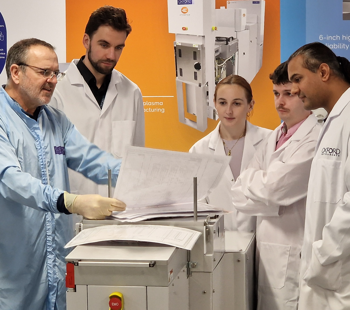
We work closely with our customers to explore what’s possible, developing and refining process “recipes” tailored to their specific challenges.
This includes:
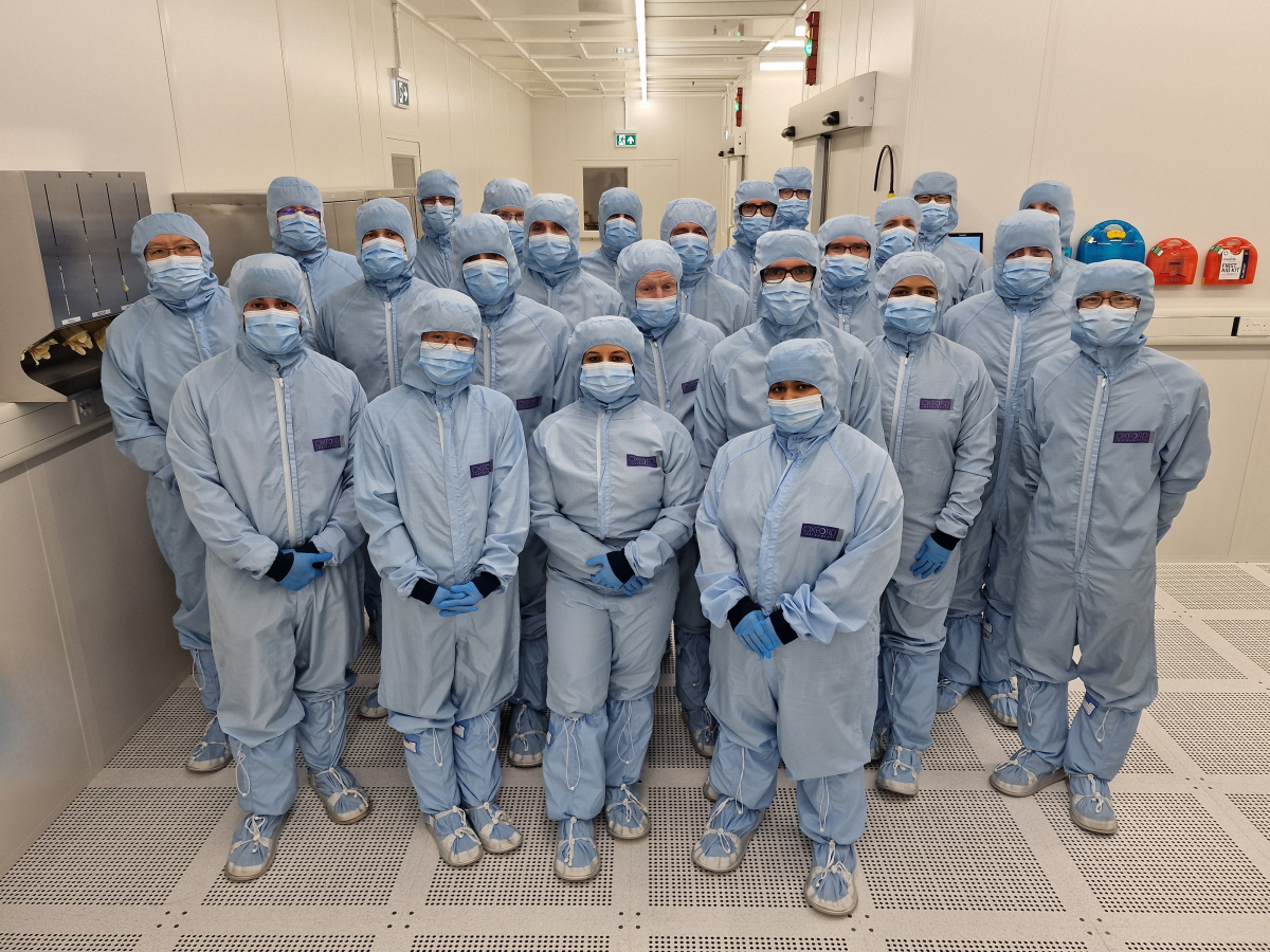
Built through decades of collaboration with academic and research organisations, our approach combines deep technical expertise with a can-do mindset—turning new ideas into working solutions.
As semiconductor technologies move towards commercialisation, the ability to scale becomes the defining factor for success.
We design our platforms with production in mind—enabling:
Our solutions support customers operating at every stage—from pilot lines to full-scale fabrication—delivering the performance, reliability, and consistency required in high-volume environments.
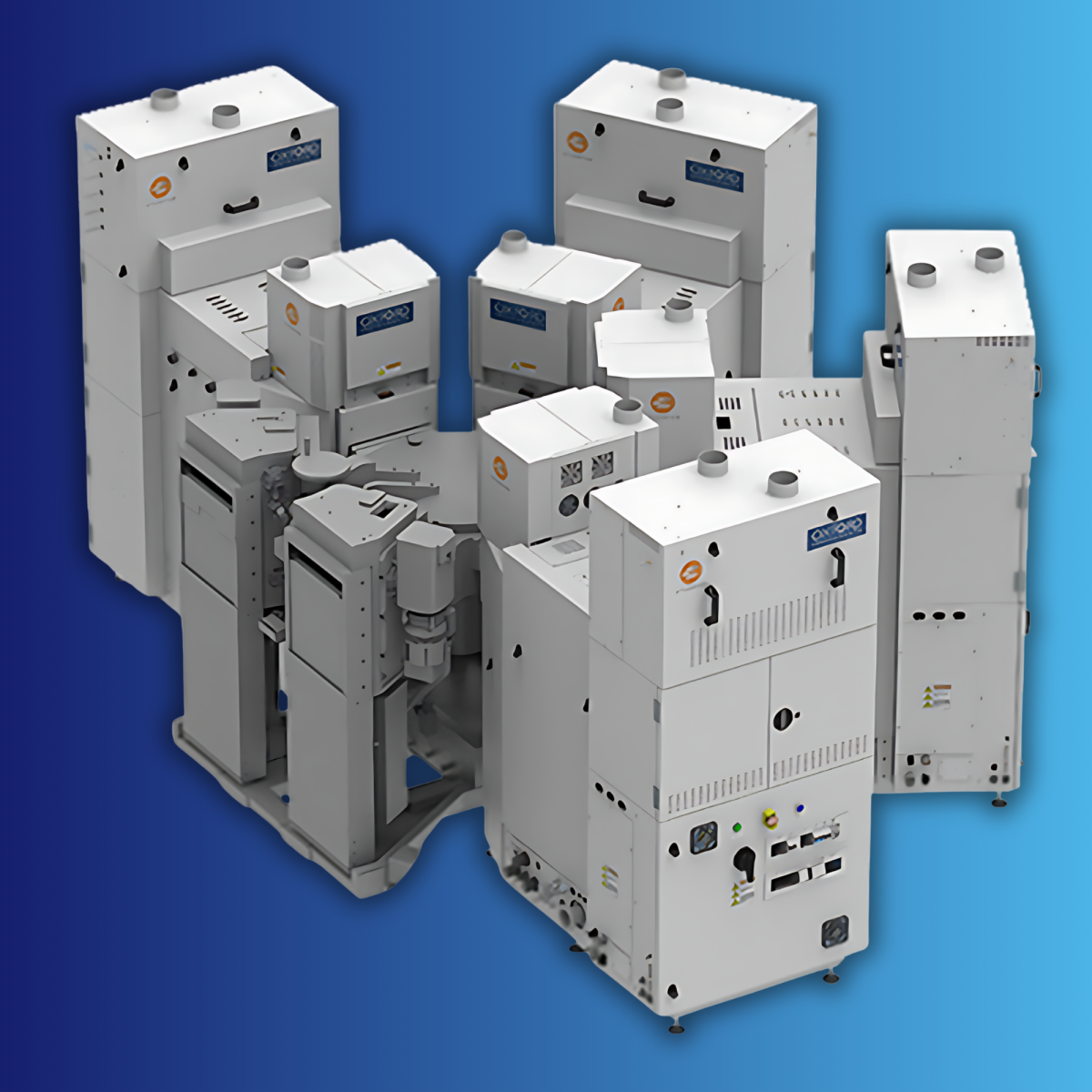
Proven production platforms such as Atomfab demonstrate this capability, with the ability to process thousands of wafers per month while maintaining precision and uniformity.
Our technology is used by customers operating at the forefront of semiconductor manufacturing, from research organisations and pilot lines to high-volume production environments.
Explore our latest news to discover how we are working with leading companies across the sector to deliver advanced process solutions at scale.
Read our latest press releases to learn more about customer collaborations, technology deployments and production successes.
Explore press releases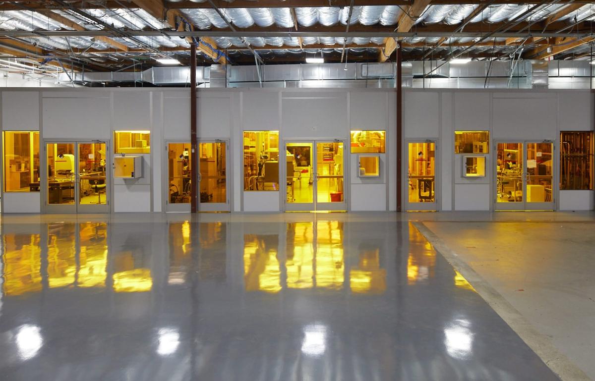
Our technologies support some of the most advanced and high-growth areas in the semiconductor industry, including:
Across these areas, our expertise in materials, interfaces, and process control helps unlock new device capabilities and accelerate technology development—turning emerging concepts into technologies that perform in the real world.
Explore applications
Our expertise is built on advanced plasma processing and atomic-scale engineering, where device performance is defined by materials and interfaces.
Our capabilities include:
These technologies allow customers to achieve:
By combining precision with throughput, we help bridge the gap between experimental success and manufacturable solutions.
Explore equipment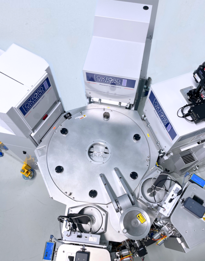
We are committed to minimising the environmental impact of our operations, products, and services—while supporting technologies that contribute to a more sustainable and efficient world.
Our focus includes:
Energy and climate
Resource efficiency and waste
Biodiversity and environment
We continuously evolve how we operate—reducing environmental impact while improving how we support our people, customers, and communities.
Smarter ways of working
Sustainable infrastructure and transport
People and culture
Together, these approaches help us reduce impact, work more efficiently, and support our customers in achieving their own sustainability goals.
We are proud to hold ISO 9001, ISO 45001 and ISO 14001 certifications, demonstrating our commitment to quality management, occupational health and safety, and environmental responsibility. These internationally recognised standards ensure we deliver consistent, reliable services while continually improving our processes.

Oxford Instruments Plasma Technology is part of Oxford Instruments plc, a UK-based FTSE 250 company with a global reputation for enabling breakthrough science and advanced manufacturing.
With decades of experience in materials science, engineering, and plasma technology, we support customers across research, development, and production environments worldwide.
Our global presence enables us to:
Our technologies are trusted in critical environments where precision, reliability, and performance are essential—supporting customers in developing and manufacturing the semiconductor technologies that drive global progress.
Work with experts in process innovation and high-volume manufacturing to take your ideas from first recipe to full-scale deployment.
Speak with an expertHeadquartered in Bristol, UK, we operate globally, supporting customers across key semiconductor markets worldwide.
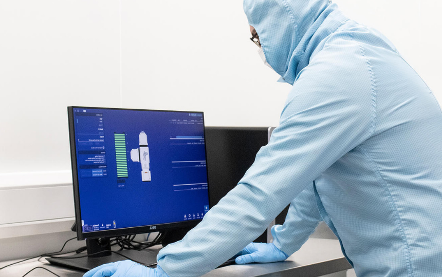
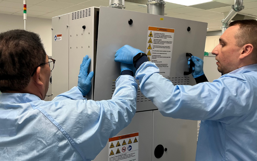
Oxford Instruments is committed to providing a comprehensive, flexible and reliable global customer support. We offer excellent quality service throughout the life of your system.
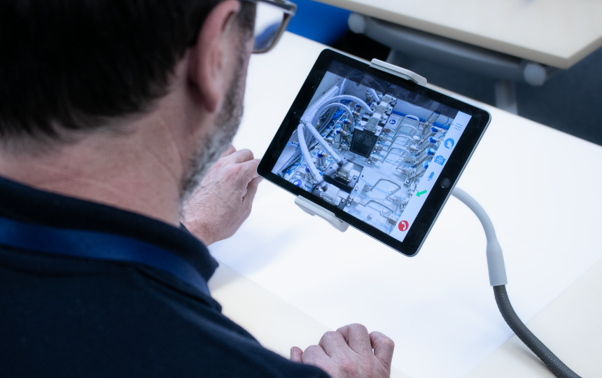
PTIQ is the latest intelligent software solution for PlasmaPro and Ionfab processing equipment.
At Oxford Instruments Plasma Technology, we offer a wide range of technical training courses designed to suit all skill levels and needs.

© Oxford Instruments 2026