1. Introduction
GaN on SiC RF devices are becoming increasingly important to realise the efficient high frequency devices required for today's communications. The high electron mobility of the AlGaN/GaN 2DEG enables fast switching times with low power loss. Building these devices requires precise control of plasma processing, without this knowledge device lifetime and performance will be compromised. Oxford Instruments Plasma Technology delivers the solutions through advanced technology and process know-how.
2. Device Structure
GaN based RF devices offer many advantages over other materials such as switching speed and power density. The intrinsic material properties of GaN such as wide band gap, high electron mobility, high thermal conductivity and high breakdown voltage make it a good performance choice for high power high frequency devices. Native GaN substrates, however, are very expensive and are likely to remain so for the foreseeable future due to technological barriers. The substrate choices for GaN RF are currently between Si and SiC.
Si is cheap and widely available upto 300mm wafer diameter but it has drawbacks in that the lattice mismatch and co-efficient of thermal expansion difference are large which creates defects in the GaN grown on top and high wafer stress unless complex stress relief structures are incorporated.
While SiC has a closer lattice match it is still relatively expensive and wafers are limited to 150mm diameter. If considerations of grown GaN quality and substrate costs are balanced SiC is the substrate of choice for many applications. However, SiC as commonly used for substrates is semi-insulating which adds certain process requirements into the device fabrication chain, specifically a through wafer via to enable a backside contact to the active device.
Figure 1 is a schematic of the finished device. It shows the features specific to the geometry of a GaN RF device grown on a SiC substrate. Many of these features require plasma processing to be realised. Oxford Instruments as a provider of advanced plasma processing tools enables these process steps.
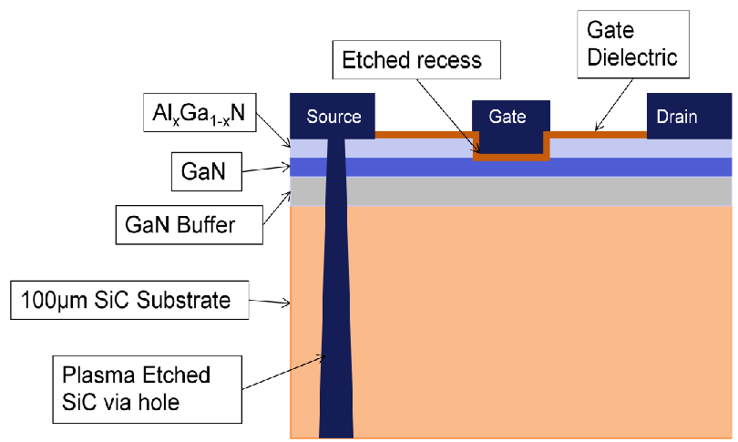 Fig. 1 — GaN based RF Device detail
Figure 2 is a typical process flow for making these devices with the plasma processing steps specifically highlighted.
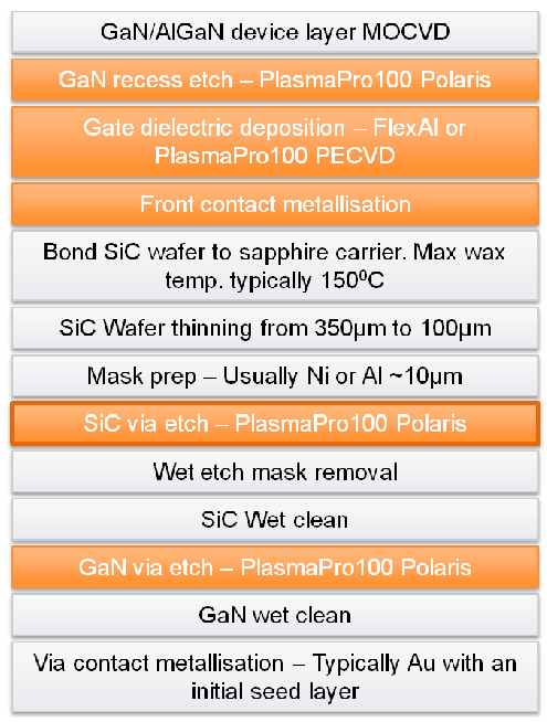 Fig. 2 — Manufacturing process flow; highlighted items use plasma processing tools
3. Plasma Processing Steps
3.1 GaN Recess Etch
In order for a normally off HEMT device to be realised with both low leakage current and minimal on resistance the AlGaN layer needs to be etched down to the underlying GaN. This AlGaN layer is thin, typically 20–30nm and there is no inherent selectivity to GaN for a classic etch process. Therefore an extremely uniform, low etch rate is essential to allow for the depth accuracy to be achieved across a complete wafer.
The AlGaN process is performed using an RIE-ICP tool, a chamber schematic is shown in figure 3. RIE-ICP allows the independent control of ion density and the accelerating voltage that the sample experiences as placed on the lower electrode. The advanced plasma source and Automatic Matching Unit (AMU) on the PlasmaPro100 Cobra300 allows the plasma density to be controlled repeatedly at very low levels. With a low power chlorine based plasma the etch rate is reduced to <3nm/min while uniformity across a 6" wafer is <+/-4%. This etch rate ensures depth control is at the nm level required for optimal device performance. While surface roughness of the etched surface only shows an increase in 0.02nm RMS. Figure 4 shows an AFM measurement of the pre and post-etch surface.
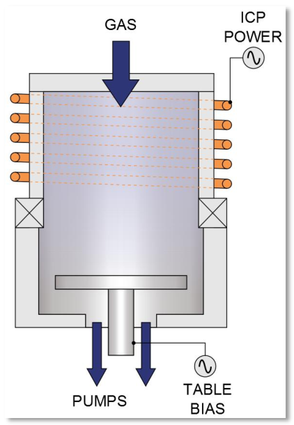 Fig. 3 — RIE-ICP tool used for plasma etching the AlGaN layer
A new method that can be applied to etch this layer with great accuracy is Atomic Layer Etching (ALE). Here a fast switching technique is used to alternate between a step that creates a very specific surface compound with the top layer of atoms and an etching step which removes this layer of compound only leaving the underlying atoms untouched. Through this technique very high control and low damage can be achieved with repeatable etch rates down to 1.8nm/min. The tool is a modified version of the RIE-ICP with faster acting valves and switching control that enables the rapid alternating between dose, purge, etch and pump out steps.
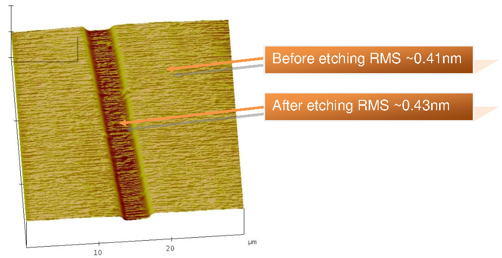 Fig. 4 — RMS Roughness of post etched surface (before etching RMS ~0.41nm; after etching RMS ~0.43nm)
3.2 ALD Dielectric
Atomic Layer Deposition (ALD) is considered for deposition of the gate dielectric and related passivation layers, due to its excellent growth control and ability to grow high-quality material at relatively low temperatures. One of the key issues is achieving low defect densities at the interfaces of these materials in the device, for instance in a structure as in Fig. 1. The shown recessed gate structure which allows control over the threshold voltage furthermore requires that the deposition is conformal and low damage. Several materials can be considered such as Al2O3, HfAlOx, AlN, SiNx, and even GaN itself.
To achieve a low defect density at the interface of GaN and the gate dielectric, a variety of surface treatments and cleans are considered. One possibility of doing surface treatments would be doing the treatment in situ, in the ALD tool itself. This could be a plasma surface treatment (e.g., H2, N2, NH3 plasma). Another effect that can be used is the self-cleaning effect of Al(CH3)3 (TMA), which is the typical ALD precursor for Al2O3. TMA is a reducing agent which can for instance reduce some compound semiconductor oxides, while forming Al2O3. Recently, Kerr et al. reported a combined approach using an Oxford Instruments FlexAL® ALD reactor [1]. In their work they demonstrated that doing H2 plasma exposures alternated by TMA exposures as a pre-treatment resulted in low defect density (Dit) values. For InGaAs devices, pulses of TDMAT (Ti(NMe2)4) have been employed as a pretreatment [2]. A similar approach might work for GaN devices in order to have a higher-k interface layer (e.g., have high-k TiOx at the interface instead of AlOx which is obtained after TMA pulses). In general a wide range of ALD precursors could be of interest as a pre-treatment to clean-up the native oxide on III-V materials [3].
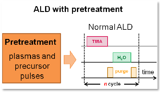 Fig. 5 — Besides the capability to run ALD processes, an ALD tool can be used to run a variety of treatments. For instance pulses of plasma and precursor before an ALD process can be used to clean and condition a surface for low defect density and effective ALD nucleation.
Another approach is the growing of ALD nitride interface layers such as reported by Liu et al. using an Oxford Instruments OpAL® reactor [4, 5]. In their work they demonstrated epitaxial growth of 4nm AlN on GaN on which they deposited 10nm ALD Al2O3 resulting in a dielectric stack with excellent device performance. Similarly, N2 plasma can be used to create a thin nitride interlayer [6, 7]. Potentially it might be of interest to mix the AlN with GaN to re-grow part of the AlGaN. GaN with relatively low impurity values was obtained as can be seen in figure 6, where it was found that the plasma parameters were most important. Such ALD GaN processes could be relevant for future GaN device structures.
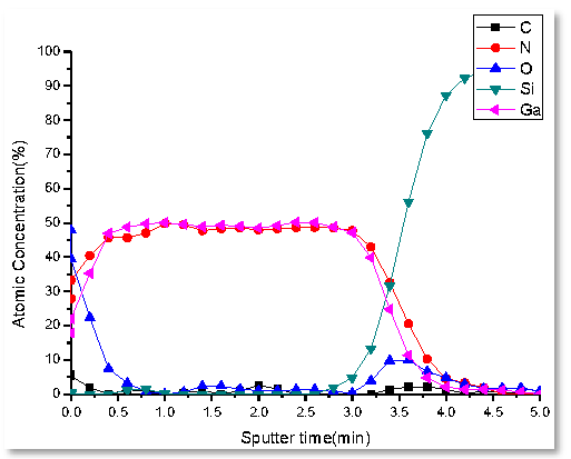 Fig. 6 — An AES depth profile of ALD GaN film. Close to stoichiometric GaN was obtained using 350°C table temperature, and an ALD cycle using triethyl gallium (TEGa) and 10 s H2/N2 plasma (30:10) at 400W power at 5 mTorr gas pressure.
Generally the effect of the plasma on the surface can depend on the composition and characteristics of the plasma. O2 plasmas are known to be able to oxidize GaN and adversely affect the threshold voltage [8]. As discussed; H2, N2, and NH3 plasma can actually be used to reduce surface damage. Generally, varying pressure and plasma power in ICP allows the minimization of the ion energy and flux [9, 10]. Note that ion energies of ~20 eV need not negatively affect device performance. For instance, the H2 plasma pretreatments performed by Kerr et al. [1], led to low defect densities while the plasma power of 100 W and plasma pressure of 20 mTorr indicate such ion energies.
3.3 SiN Gate Dielectric
SiN can be used as an alternative gate passivation material, deposited using Plasma Enhanced Chemical Vapour Deposition (PECVD) or Inductively Coupled Plasma Chemical Vapour Deposition (ICP CVD) shown in figures 7 and 8 respectively.
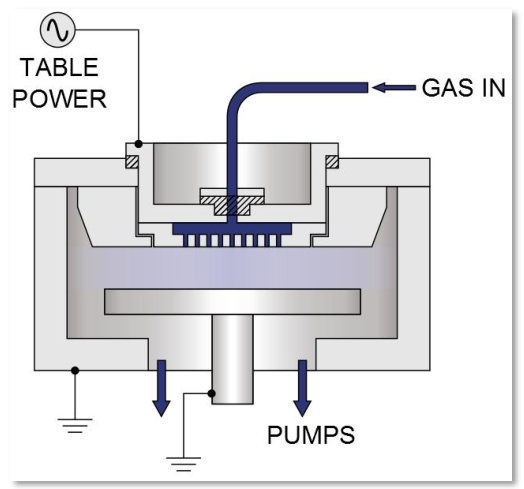 Fig. 7 — PECVD tool allowing high density film deposition
Using a combination of SiH4, NH3 and N2 gases a high quality film layer can be grown at typical temperatures of 300°C. Film stress can also be accurately controlled using a combination of 2 frequencies to create the plasma which ensures excellent adhesion of the film. ICP-CVD utilises the higher density plasma that can be created within the ICP source. Higher density plasma delivers high film quality: high VBD, low BOE. At a lower temperature, for example at 150°C the film has a VBD of 7MV/cm whereas a PECVD film deposited at 300°C has VBD 5MV.
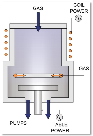 Fig. 8 — ICP CVD Schematic, high quality films at low temperature
3.4 SiC Via Hole Etch
After the device structure is formed on the front of the wafer in order to form a backside contact it is necessary to get through the SiC substrate. The first step of this is to mount the wafer front side down on a sapphire carrier using a wax material, this is important as the wax will have an upper temperature stability limit of ~150°C which has implications for the subsequent processing. The wafer is then thinned by Chemical Mechanical Polishing (CMP) from its original thickness of >350μm down to 100μm. Then a hard mask, typically Ni, is deposited and patterned to form the etch mask for the SiC via etch process. Following the CMP steps there are some surface residues which if not dealt with correctly would form spikes or grass during the SiC etch process, this grass would cause device failure so it is essential that it is avoided. Oxford Instruments has developed a plasma surface treatment and etch process which ensures these residues are removed. Device lifetimes are then improved as the etch surface and sidewalls are smooth and metallisation shows no defects.
The mounted wafer is transferred into the PlasmaPro100 Polaris tool where it is clamped to the lower electrode using Oxford Instruments unique, patented, Electrostatic Clamp (ESC) technology. The ESC designed by OI is capable of clamping both conducting and non-conducting substrates. This capability is important as the sapphire substrate is insulating which makes a strong clamping force difficult for standard ESC technology. Clamping is essential because of the stability of SiC, its strongly bonded material makes it difficult to etch and requires a high density plasma and accelerating voltage to produce the etch rates needed for low Cost of Ownership (COO). Clamping is the mechanism that is used to introduce cooling to the wafer, a pressure of He gas is maintained between the wafer and the electrode which acts as a heat transfer medium. The electrode itself has active cooling so the wafer is cooled via the He layer. Without efficient clamping sufficient He backside pressure can not be maintained without the wafer moving. Cooling is essential because of the temperature limitation of the wax bonding the wafer to the carrier, if the wafer was not cooled the wax would melt under the high plasma powers. So a chain of technology is required to produce high etch rates for low COO: clamping of non-conducting substrates; high plasma powers and efficient cooling. All these have been developed for the PlasmaPro100 Polaris tool enabling a fast, uniform high quality etch of the SiC via. The etch process itself is based on a combination of SF6 and O2 gases in the correct ratio to provide volatile etch by-products; table 1 shows the results achieved with an optimised process.
| Parameter | Result |
|---|
| Etch Rate (μm/min) | > 1.2 |
| Depth (μm) | >100 |
| Selectivity to Ni | > 20:1 |
| Uniformity within wafer (+/- %) | < 3 at 3mm edge exclusion |
| Reproducibility (+/- %) | < 4 |
| Particles (>0.5 μm) / cm² | <1 |
| Edge Exclusion (mm) | 3 mm |
| Sidewall Angle /° (mask dependent) | >88° |
Figure 9 shows the excellent profile achieved with smooth sidewalls and etch surface.
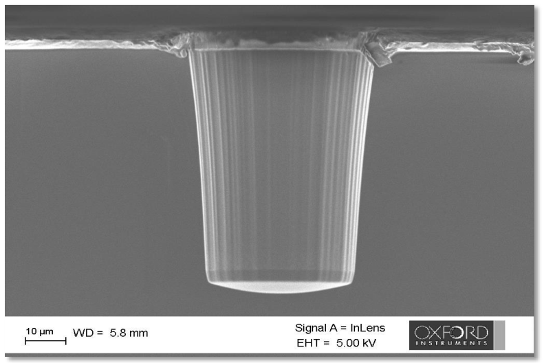 Fig. 9 — SiC via etched using RIE-ICP plasma
The main SiC etch is an aggressive high power recipe if the same recipe were to be used on reaching the underlying GaN layer this high power process would also etch the GaN surface causing pitting. A 'soft landing' step is therefore recommended. The recipe can be set-up to incorporate these parameter changes automatically and the AMU hardware positions set for these conditions so that the plasma is fully optimised in the minimum time. The new recipe is designed for high selectivity to GaN, around 50:1, so that the GaN surface has minimal etch and damage during the SiC process. The SiC etch rate is 0.3μm/min, it also allows for all the SiC to be removed across the whole wafer making sure that the next GaN etch step is clean and smooth, as shown in figure 10.
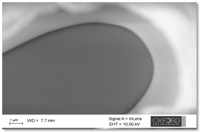 Fig. 10 — Smooth GaN surface after all the SiC has been etched from the via hole
During the etch process the Ni mask is sputtered from the surface and is re-deposited on the wafer, including the exposed SiC, and the chamber. It is therefore important to manage the level of re-deposition on the chamber furniture in order to maintain low particle levels for as long as possible.
Post etch there is a plug of this re-deposited Ni material on the sidewalls of the via, this is typically removed using a wet clean process, HNO3 for example.
3.5 GaN Via
Now that the GaN layer is exposed we have to etch through this and the active layers to reach the metal front side contact. We use a BCl3 based plasma to etch the GaN/AlGaN structure and again it is performed in the PlasmaPro100 Polaris tool. The flexibility of the source and the AMU means that a repeatable, low power process for GaN can be set up without compromise on performance.
Etch rates of 0.3μm/min are reached through the Nitride based materials until the metal contact is reached.
4. Summary
GaN RF devices have been shown to offer real performance advantages over the current technology. Improvements in manufacturing efficiency and the performance of these devices will help their widespread adoption; plasma processing has a huge part to play in both of these. Oxford Instruments Plasma Technology has a wealth of experience around Compound Semiconductor device manufacture and the right tool set for the plasma needs of GaN devices.
5. Acknowledgements
The authors would like to thank the researchers at Hong Kong University of Science and Technology (HKUST), UC San Diego and UC Santa Barbara for their relevant work using Oxford Instruments ALD equipment.
6. References
- Kerr et al., J. Chem. Phys. 141, 104702 (2014)
- Chobpattana et al., J. Appl. Phys 116, 124104 (2014)
- Klejna and Elliott, Chem. Mater. 26, 2427 (2014)
- Liu et al., IEEE Electron Device Lett. 34, 1106 (2013)
- Liu et al., Phys. Status Solidi C 11, 953 (2014)
- Yang et al., IEEE Electron Device Lett. 34, 1497 (2013)
- Chen et al., Phys. Status Solidi A 212, 1059 (2014)
- Ozaki et al., CS MANTECH Conf. Apr. 23rd - 26th, 2012, Boston, USA
- Profijt et al., J. Electrochem. Soc. 158, G88 (2011)
- Profijt et al., J. Vac. Sci. Technol. A 31, 01A106 (2013)

