Introduction
Failure analysis (FA) is an essential part of semiconductor device manufacturing — it is the detective work that roots out defects and helps maintain the consistent, reliable manufacture of high quality components.
In this white paper we present a suite of plasma processing tools for FA with the aim of providing practical guidance as to their suitability for different tasks. One way of uncovering a fault and diagnosing its origin is the progressive and precise removal of various device layers to expose the embedded circuit structure. The density of modern integrated circuits (ICs) means that wet etching processes are no longer viable for this forensic task and they have now been displaced by more sophisticated plasma processing techniques. Plasma etching allows accurate and reproducible delayering, while plasma deposition enables the conformal coating of features of interest, a technique called decoration — this provides the sharp contrast required for productive imaging.
The merits of plasma enhanced (PE) etching, reactive ion etching (RIE) and inductively coupled plasma (ICP) etching are considered for the removal of materials routinely encountered in FA. Plasma enhanced chemical vapour deposition (PECVD) and atomic layer deposition (ALD) are compared for decoration applications.
Establishing Requirements for Effective FA
Conducting effective FA analysis is a quite different task from developing a fixed manufacturing process. In the FA lab with each new case the structure and materials encountered can vary considerably from device to device, wafer to wafer. With FA each new case calls for a uniquely tailored investigation, this creates a requirement for a set of flexible tools that can be used to:
- Carefully deconstruct the device
- Characterise the elemental chemistry of the device, down to grain scale
- Enhance the contrast of exposed surface allowing a more detailed analysis
- Visualise, in detail, exposed structures and surfaces
Oxford Instruments offers technology that addresses each of these issues, thereby providing a complete solution for FA. Here the focus is on one element of this package — plasma processing techniques — their application and value.
Figure 1 shows a typical structure of a device constructed in accordance with modern protocols for Very Large Scale Integration (VLSI). The drive towards smaller, faster more powerful devices is directly responsible for the complex, multi-layered design of modern chips and creates an intricate structure. In order to perform FA on such chips each layer must be carefully removed in the search for a defect area which can be tested to identify the cause of the failure. The FA investigation is applied to full wafers (up to 300 mm in diameter), to a bare die — a piece of a wafer — or even to an unpackaged die.
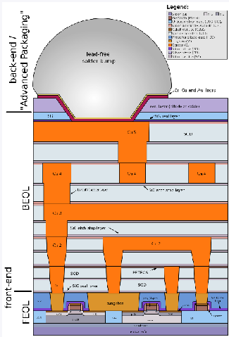
Fig. 1 — Since Very-Large-Scale-Integration (VLSI) began in the 1970s IC designs have become increasingly dense and complex, creating a significant challenge for FA. Courtesy of Cepheiden.
A wide range of materials can be encountered; however, some are particularly widely used and common to a sizeable number of devices. These include polyimide, for coating and protection, silicon nitride (SiNx), for passivation, and silicon oxide (SiO2) or variants thereof — the most frequently used intermetal dielectric (IMD).
A primary requirement in FA is to delayer the sample without lifting or damaging the metal patterned circuitry, usually copper or aluminium ‘tracks’, to maintain its integrity for detailed study and testing. The sequential etching required to achieve this goal gets progressively more challenging with each layer, as access to underlying layers becomes restricted by an emerging mesh of exposed tracks. Maintaining verticality as aspect ratios increase is difficult but important as any undercut can cause tracks to lift while a positive slope would close any gaps and mean that lower layers would not be reached. The planar surface of the structure must be preserved with each sequential step to enable further investigation.
As the analysis proceeds it may also be necessary to remove some of the metal structure to gain access to the area beneath and allow the etching away of the barrier layers beneath the track. To prevent diffusion of the metal layer into the surrounding dielectric, metal tracks are often printed onto an underlying barrier layer of, for example, titanium nitride (TiN) or tungsten; an upper barrier layer may also be applied to seal the track. These layers must also be removed in order to ensure the smooth removal of the IMDs.
All these deconstruction goals can be realised via the knowledgeable application of a range of plasma etching tools.
Layer Removal — Plasma Processing Tools for Etching
Plasma etching techniques combine flexibility with high performance for FA applications. Clean, non-toxic and non-hazardous, they enable uniform delayering of all the types of samples routinely encountered. A basic understanding of the three most applicable etching techniques supports an appreciation of their differences and an understanding of which to select for a given task.
Plasma Enhanced Etching / Reactive Ion Etching — Switch Between Isotropy and Anisotropy as Requirements Change
The equipment used for PE and RIE are closely similar, to the extent that some units, such as the Plasma Pro™ 80, offer dual mode operation, allowing the user to switch between techniques depending on requirements. Figure 2 shows a schematic of a unit set up for RIE (left) and PE (right) along with the etching profiles delivered.
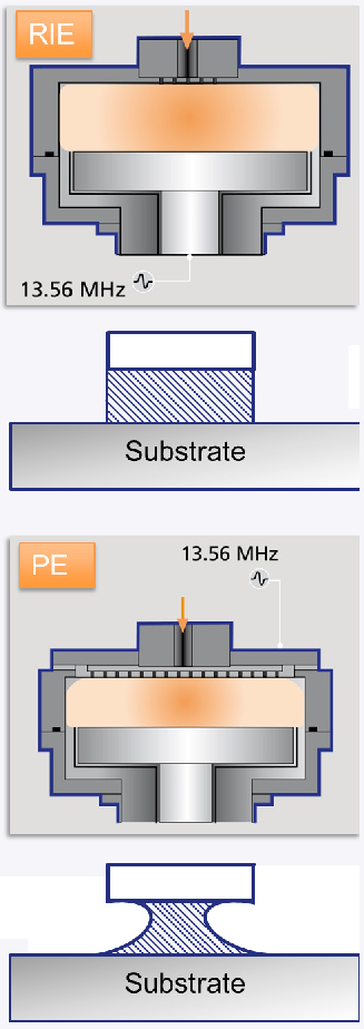
Fig. 2 — A dual mode unit for PE and RIE enables both anisotropic and isotropic etching.
With PE, gas enters the chamber through a showerhead; the showerhead has RF power supplied to it which initiates formation of the plasma. The substrate sits on a lower grounded electrode and is essentially ‘bathed’ in the plasma in an analogous way to liquid submersion in a wet etching process. The resulting etch is therefore isotropic with etching occurring equally energetically wherever the plasma can access the substrate. An undercut profile associated with plasma penetrating beneath a feature is shown.
The critical difference with RIE is that the bottom electrode is now RF powered rather than the top. Gas is still introduced via the top showerhead, but plasma is now initiated by the RF power applied at the lower electrode. This induces a negative self-bias on the table that makes the etching process directional. Positive ions are accelerated towards the substrate and impact with an energy that is dependent on the strength of the DC bias applied which typically lies in the region of 100–800 V. Putting more power into the electrode creates a higher bias and will deliver a higher etch rate but increases the risk of unintended damage. However, with the correct adjustment of parameters, the etch is now anisotropic — material is removed in one direction, giving the vertical profile shown.
While the process chemistries applied with PE and RIE are frequently the same, and both are operated at relatively low temperatures (with the specimen usually maintained in the range 10 to 80°C), other process conditions are somewhat different. PE processes tend to be operated at a substantially higher pressure — at around 0.2–1 Torr compared with the 5–500 mTorr used for RIE — and markedly lower power density, 0.02–0.1 c.f. 0.1–1.5 W/cm2. As a result, PE is associated with less risk of substrate damage, an important benefit. On the other hand, the isotropic nature of PE is undoubtedly an issue for many FA requirements, with RIE offering the anisotropy required.
The table below summarises the performance obtained with RIE and PE of certain materials, along with selectivities of the most relevance for FA based on proximity to other materials in a device. This performance is achieved using standard process chemistries with CF4, CHF3, O2 and Ar gases. Fluoride chemistries are particularly beneficial for FA because the methyl fluoride compounds produced during the etch form a protective layer on the metal tracks. By carefully balancing the condensation process that produces this layer with the rate of removal of, for example, SiO2, it is possible to delayer the device while maintaining the sharp, well-defined edges of the metal tracks.
It is notable that the reported etch rates are far lower than those associated with many manufacturing applications while selectivity figures are relatively high. This reflects the exacting requirements of FA tasks. In each case excellent run-to-run reproducibility is achieved in terms of etch rate, selectivity, uniformity across the wafer and profile.
| Process | Mode | Etch Rate (Å/min) | Selectivity |
| Polyimide | RIE | >1000 | to SiNx > 15:1 |
| Depassivation (SiNx) | PE | >500 | to SiOx > 7:1 |
| SiOx (BPSG; TEOS) | RIE | >250 | to Poly-Si > 7:1 |
Table 1: Performance metrics for RIE and PE processes in FA applications. Data generated using a Plasma Pro 80 [where BPSG is borophosphosilicate glass which is routinely used as an IMD and TEOS is Tetraethyl Orthosilicate and used to identify SiO
2 produced from this precursor].
Inductively Coupled Plasma Enhanced Reactive Ion Etching — Access Higher Etch Rates with Minimal Risk of Damage/Sputtering
In ICP-RIE an ICP source is used to generate high density plasma compared to standard RIE. Specific gases are fed in at the top of the vacuum chamber and a plasma is struck as they pass through a powered coil. Energy is transferred into the plasma by a process of inductive coupling. Oxford Instruments Plasma Technology has a specific design that eliminates capacitive coupling, with an electrostatic shield; this delivers superior performance by preventing sputtering of the ceramic tube in which the plasma is generated, thereby removing a source of contamination in the etching process. A second power supply is used to induce RF biasing across the substrate table (see figure 3).
Crucially, this configuration enables the independent manipulation of ion density and energy — which in conventional RIE are controlled with the same single RF source — allowing etch rates to be enhanced without any accompanying increase in bias. With ICP-RIE ion density can be tuned to maximise etch rate, through the manipulation of RF power to the coil, while ion energy, which is controlled via RF power to the table, is kept low to enhance selectivity and reduce substrate damage. Furthermore, by achieving higher plasma densities at lower operating pressure (~1–200 mTorr), ICP-RIE allows better selectivity control, more directional etching and better profile maintenance than RIE. Operating temperatures are higher than with conventional RIE, but modern ICP-RIE systems incorporate active sample cooling/heating that ensures excellent wafer temperature control.
Though ICP-RIE is a more complex process than RIE, the benefits it offers have considerable value in certain FA applications and some units, such as the Plasma Pro 80 Cobra, offer the functionality to switch between the two techniques. ICP-RIE delivers high etch rates (e.g. >100 nm/min for SiO2 c.f. ~25 nm/min with RIE) for a wide range of materials, and is particularly useful for the low damage, high aspect ratio etching required to expose the deeper layers of a device and for the analysis of bare dies and packaged devices. When using RIE with a packaged device the DC bias is typically reduced to minimise sputtering of the packaging material, but this simultaneously reduces etch rates. With ICP-RIE, live packaged devices can be etched at a relatively high rate with a DC bias as low as 60 V, even remaining functional after etching. That said, RIE remains the ‘go to’, lower cost option for less demanding etches.
The table below summarises the ICP-RIE etch performance that can be achieved for a wide range of materials including certain proprietary products such as SiLK, a spin-on hydrocarbon semiconductor dielectric (The Dow Chemical Company), and Black Diamond (Applied Materials) and Coral (Lam Research), both of which are low-k (dielectric constant) SiOC:H dielectrics used because of their enhanced properties relative to SiO2.
| Process | Etch Rate (Å/min) | Selectivity | Uniformity (50 mm wafer) |
| Polyimide | >5000 | >15:1 to SiNx | < ±5% |
| SiNx Depassivation | ~1000 | ~1.5:1 to TEOS or SiC | < ±5% |
| SiC | >1000 | ~1.4:1 to TEOS; ~0.7:1 to low-k dielectrics | |
| SiOx ILD (BPSG, TEOS) | >1000 | ~0.5:1 to low-k dielectrics; ~0.7:1 to SiC | < ±5% |
| SiOC:H low-k dielectrics, e.g. "Coral" "Black Diamond" | >1500 | ~2:1 to TEOS; ~1.3:1 to SiC | < ±5% |
| "Silk" spin-on resin | >3500 | | < ±5% |
| SiOx with higher selectivity to Nitride (RIE mode) | ~200 | 7:1 | |
| Bulk Si removal | ~50000 | >100:1 to SiO2 | |
Table 2: Performance metrics for ICP-RIE processes show its broad applicability for FA. Data generated using a Plasma Pro 80 Cobra using standard fluoride-based process chemistries.
Identifying the optimum plasma processing solution for a given stage of a FA relies on determining suitable process chemistry and confirming that the achievable performance is well-matched to requirements. The following examples illustrate in greater detail what the three etching techniques can deliver, using specific process chemistries.
Example 1: Polyimide, IMD and Passivation Layer Removal Using a Combination of RIE and PE
In this example, three discrete etching steps have been carried out, all using a standard, fluoride-based process gas mixture (CF4, CHF3, O2, Ar). In the first step the polyimide outer coating of the device has been removed using RIE. RIE can be tuned to be fast and efficient for this step since there is negligible risk of critical damage with no metal exposed. Similarly, the second step, removal of the SiNx passivation layer can be realised using PE because there is no risk of the plasma penetrating beneath the as yet unexposed metal tracks. However, once the passivation layer has been removed, RIE becomes the technique of choice because it is now important to ensure an anisotropic etch with no lifting of or damage to the metal tracks.
The rates and selectivities achieved in these etches are as reported in Table 1 but they were carried out using a different unit, a Plasma Pro 800, which is suitable for wafers up to 300 mm in size. Further evidence of the quality of the etching process is provided by the uniformity data and associated images (see figure 5). For example, variability of less than +/- 5% is observed across the 300 mm wafer in the IMD etch, highlighting the ability of the etch process to maintain the planar structure of the device, readying it for further delayering.
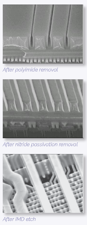
Fig. 4 — The sequential application of RIE – PE – RIE allows precise removal of the polyimide, passivation and IMD layers of the device, respectively.
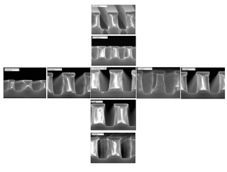
Fig. 5 — Excellent uniformity ensures that each layer is cleanly removed prior to subsequent analysis/delayering.
Example 2: Polyimide, Passivation and IMD Layer Removal by ICP-RIE
Figure 6 shows images of an analogous delayering to Example 1, this time realised using ICP-RIE for all three steps. Standard fluoride process chemistry was applied and the etch rates and selectivities achieved are as shown in Table 2. Etch rates for all three steps are higher than with RIE but on the whole selectivity is not as high, the exception being for the removal of polyimide which is removed with very high selectivity relative to SiNx.
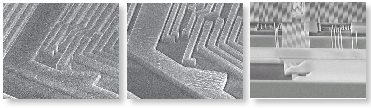
Fig. 6 — ICP-RIE delivers higher etch rates than RIE for the removal of polyimide (left), SiN x passivation (centre) and IMD layers (right).
In these etches a laser interferometer was used to detect the endpoint for the etch and prevent over-etching. This in-process monitoring tool detects a change in the material through which the etch is proceeding from shifts in refractive index, providing clear evidence of progress through successive layers (see figure 7). It can therefore be extremely useful for FA applications, where precise control of etch depth is required.
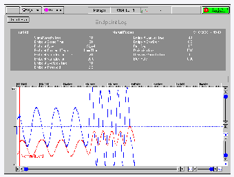
Fig. 7 — An in-line laser interferometer detects changes in the material through which an etch is proceeding, helping to prevent over-etching.
Example 3: RIE Sputtering Metal Etch Process to ICP Mode Cu Etch Process
In order to reach deeper and deeper layers it is often necessary to etch the metal tracks cleanly; this ensures that the metal does not act as a mask for further etching. Some metals do not readily form volatile etch products and are sputtered using Ar plasma chemistry. This can etch a range of metals at acceptable rates (see table 3), simultaneously maintaining the profile of the surrounding features. Other metals such as Cu will form volatile etch products and process solutions have been specifically developed for these.
| Parameter | Value |
| Process gases | Ar |
| Ag, Al, Au, Cu etch rates | >20 nm/min |
| Pd, Pt etch rates | >5 nm/min |
| Ni, NiFe, NiCr etch rates | >3 nm/min |
| Uniformity | < ±5% |
| Selectivity OR | >0.5:1 |
| Profile | >65° |
Table 3: RIE, with Ar process chemistry, is a useful tool for metal etching to remove structures encountered during the deconstruction process.
Example 4: Removal of the Metallisation Barrier Layer
Table 4 and Figure 8 show the results of using RIE to etch away the metallisation barrier layer material associated with the metal circuitry within a device. Here, the process gases used are SiCl4 and Cl2 and a load lock system or N2 purge glove box is required. A load lock system maintains the chamber of the processing unit under vacuum at all times ensuring the good repeatability and use of corrosive gases such as chlorine. The use of a N2 purged glove box is an alternative approach but does not provide the same assurance of containment. Using a relatively low etch rate the TiN is removed to leave a smooth, residue-free substrate and a sidewall with a well-defined profile. Uniformity across the wafer is high.
| Parameter | Value |
| Process gases | SiCl4 and Cl2 |
| TiN etch rate | >40 nm/min |
| Uniformity | < ±5% on 100 mm |
| Selectivity TiN: PR | >1:1 |
| Selectivity TiN: SiO2 | >2:1 |
| Profile | >70° (PR dependent) |
| Substrate and sidewall | Smooth, residue free |
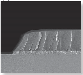
Fig. 8 — RIE, with chloride process chemistry, enables the successful removal of TiN barrier layers.
Boosting the Performance of RIE — Focused Plasma
Some RIE tools have a plasma focusing apparatus which, as the name suggests, focuses the plasma on a specific, reduced area of the table. Such apparatus can be used to access ICP-RIE levels of performance with an RIE tool, though only over a relatively small working area. For example, with plasma focused RIE the etch rate of SiO2 can be boosted to 500 nm/min over a small piece of die — 1.5 cm x 1.5 cm — compared with 25 nm/min with RIE in conventional mode and 100 nm/min with ICP-RIE. Focused plasma can therefore be very useful for enhancing the applicability of RIE tools to small die and packaged devices that might more routinely be handled with an ICP-RIE system. Heating of the device can be an issue because of the focusing effect but this can be addressed by bonding the specimen to a larger body, to provide a heat sink.
The photo above shows plasma focusing apparatus in-situ that can be used to mount different packages/pieces and boosts the performance of the Plasma Pro 80 RIE tool for different FA applications. The below SEM images show removal of the top two layers of a device, a process that took 44 minutes with conventional RIE. In contrast, on the right, all four of the top layers have been removed with no metal erosion or lifting, in just 5 minutes using plasma focused RIE.
Feature Elucidation — Etching and Deposition Techniques for Optimal Imaging
Though much of the challenge of FA is delayering without collateral damage, it is often the case that exposed features need delineation to enhance the information that can be gathered from imaging. Figure 9 shows how the application of a simple RIE decorative etch, which can be completed in just a couple of minutes, can substantially improve the quality of images gathered.
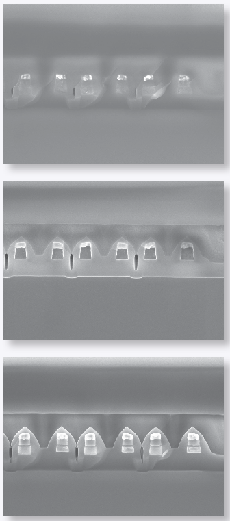
Fig. 9 — The application of a decorative RIE etch with basic fluoride process chemistry (middle and right image) reveals details that cannot be determined from the image of the unetched feature (left).
An alternative approach, depending on the feature, is to apply a coating so that it acquires greater relief and correspondingly enhanced contrast within the image. With this approach the conformality of the coating is essential — in other words the geometry of the original feature must be precisely preserved to avoid compromising the integrity of the analysis. There are two deposition techniques that can be applied here, and, as with etching, it is helpful to appreciate their strengths and limitations to make an informed choice.
PECVD — Fast, High Quality Coating for a Wide Range of Materials
PECVD is a relatively low-cost deposition technique with broad applicability that produces high quality films. The key features of a PECVD unit are shown in figure 10. Plasma is generated at the upper charged electrode with deposition occurring on the substrate surface due to reactions between radicals and ions in the plasma. Unwanted reaction by-products are pumped away. Operating pressures are typically in the region of 0.5 to 1.0 Torr and operating temperatures tend to lie in the range 90–400°C with the substrate normally maintained at a temperature ~300°C. Uniform films are produced with high density and minimal pinholing. For FA applications PECVD can be used to deposit SiO2, SiNx, SiC and a range of other materials.
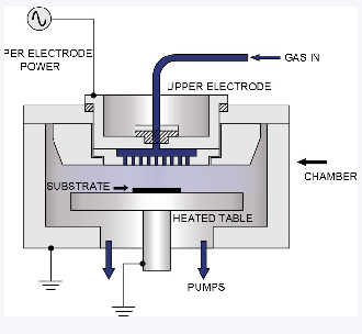
Fig. 10 — PECVD is a relatively low-cost deposition technique that can be used for a wide range of different materials.
ALD — Highly Conformal Coating, Even at the Highest Aspect Ratios
ALD proceeds by a self-limiting layer-by-layer growth mechanism that results in highly conformal films. This defining characteristic can be particularly helpful in FA applications for delineating intricate features, and accessing high aspect ratios, but more broadly ALD offers advantages over PECVD for certain materials such as Al2O3 by enabling far lower temperature deposition. Conversely ALD is the more complex, costly and slower process, which is why PECVD is the preference where it can deliver the performance required. The key features of an ALD unit are shown in figure 11.
Plasma ALD proceeds via a cyclical sequence of plasma pulses and associated purge steps. The first pulse introduces a gaseous precursor which absorbs and reacts onto the surface of the substrate, leaving a single monolayer. Unabsorbed precursor and reaction by-products are purged. A second pulse introduces the reactant that completes the deposited layer, with an associated purge completing the cycle. The repetition of these steps builds a coating or film that can be both pin-hole and particle free.
An ALD film will grow wherever the reactant(s) can penetrate but the growth mechanism, which restricts reaction at the surface to just a single layer of precursor, means that the thickness of the coating is closely controlled. ALD can therefore be used to coat complex geometries and high aspect ratios, using relatively long pulse times to enable the precursors to penetrate and effectively coat a given surface. Figure 12 shows examples of two features that have been coated to improve their contrast for imaging, one with Al2O3, the other with HfO2. Offering coating at temperatures as low as 50°C limits the diffusion of species such as Cu within the device, preserving the integrity of the surrounding device.
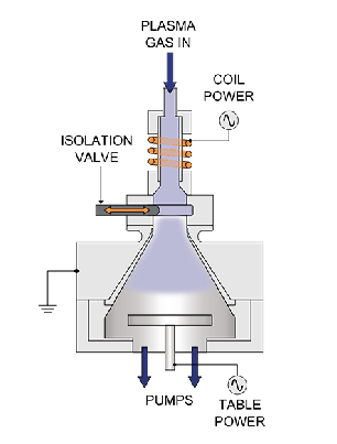
Fig. 11 — ALD enables the layer-by-layer deposition of highly conformal films, even at high aspect ratios.
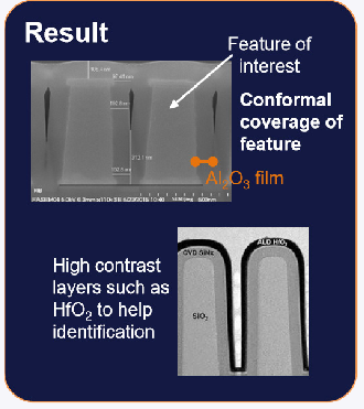
Fig. 12 — ALD enables the low temperature, conformal coverage of notable features with high contrast materials such as Al
2
O
3 and HfO
2 .
In Conclusion
Plasma processing techniques are essential techniques for modern FA, enabling the precise, reproducible delayering of a device to expose and identify a fault. A trio of etching processes enable the optimal balancing of material removal rate with the risk of substrate damage, allowing isotropic, and the increasingly precise anisotropic etching required as analysis proceeds through layers of the device. Etching can also be used to delineate features that need greater contrast, to boost the information that can be gathered during imaging, but here deposition processes have a role to play. ALD is particularly useful, because of its ability to deliver excellent conformality even at very high aspect ratios. In combination these techniques allow the forensic deconstruction of dies, devices and wafers, facilitating the FA required to eliminate problems from the manufacturing chain and ensure consistent product quality.

