Making Better Diamond and SiC Quantum Devices
Oxford Instruments is at the heart of the quantum computing revolution. We work closely with the quantum community and we understand the challenges that the community must overcome in order to achieve world class and commercially-attractive device performance. In this white paper we will review how Oxford Instruments Plasma Technology's plasma etch products can be used to solve common challenges in diamond and SiC colour centre research for quantum devices, with a focus on non-roughening thinning etches, quasi-isotropic etches, and feature etches where sidewall roughness must be minimized to maximize device performance.
Colour centres, also known as solid state defects and most closely associated with the diamond nitrogen vacancy (NV) centre, are used for a wide range of quantum applications. In the NV centre, a nitrogen atom replaces a carbon atom and a vacant site is created in the diamond structure. Researchers have studied their use for single photon sources, quantum memories, quantum repeaters, and for a variety of quantum sensing applications, including piezometers, electrometers, thermometers, and magnetometers.
Quantum magnetometry is currently the most well-developed application, with a variety of companies now working in this space. As one example, SB Quantum, part of an Innovate UK-NSERC joint funded collaboration with Oxford Instruments, is developing magnetometers for mining, infrastructure, defense, and navigation in GPS-Denied environments such as underwater. There are many other companies with launched or upcoming products for quantum microscopy, magnetometry, biomarker diagnostics, and even room temperature quantum computational accelerators. These applications typically exploit the interaction between specific material defects and magnetic fields through the Zeeman Effect.
In this whitepaper, we will describe (1) the mechanisms by which colour centres can be used as sensors, (2) device fabrication requirements and challenges in these systems, (3) Oxford Instruments' work in this area, and (4) the future of this field, including new material systems and fabrication requirements for the next generation of colour centre-based devices.
How Colour Centres Work
There are many different material systems which can be exploited to create well-behaved colour centre defects. In general, appropriate material systems have wide bandgaps, which enables an engineered defect to exist between the valence and conduction bands of the host material. It is very important for the region near the engineered defect to have a low density of states in order to avoid decoherence. Diamond is by far the most well-studied colour centre host material, followed by SiC. While there are innumerable host-defect system combinations, each with their own cocktail of physical properties, potential applications, and level of development, we will focus on two model systems: Diamond NV(-) and SiC PL6 divacancy. Although both the diamond NV(0) and NV(-) systems have been studied, by convention the NV(-) system is referred to as the NV centre. We will abide by this convention. The diamond SiV(-) and SiV(0) systems are also the subjects of intense research activity, but as of this writing SiV(-) defects are limited by an excess of phonon interactions which consequently require cryogenic temperatures for reasonable spin coherence, and the SiV(0) defect has only very recently been successfully exploited. SiV(-) colour centres have been used to create the best diamond-based single photon emitters thus far because they have more efficient emission into the Zero Phonon Line (70%) than NV centres (3%). Even more recently, the SnV(-) defect in diamond has garnered increased interest due to relatively high quantum efficiency and high spin coherence time at temperatures above 1K.
Colour centres have several advantages as compared to other systems, including relatively long coherence time, operational temperatures up to room temperature, a variety of optical operational frequencies, and all the advantages inherent to any solid state system, such as compatibility with well-developed tools for lithography, etch, and thin film deposition. A colour centre itself is quite simple: it is a point defect in a crystalline material. The point defect is usually associated with electrons or holes that are trapped out of their typical position. In the diamond NV centre, the typical diamond C-C lattice is disrupted by the substitution of a nitrogen atom and an adjacent vacancy in place of two neighboring carbon atoms. Proper surface termination is typically sufficient to maintain the NV(-) state, though a bias voltage can also be used. Defects are present at some level in natural and CVD-grown diamond, but most research takes advantage of materials engineering techniques to increase the quality of NV centres while reducing their overall density. Isotopic purification and control of CVD-grown diamond is important for many applications, and there has also been quite a bit of work undertaken to control the positions of defects through the use of techniques such as ion implantation, delta doping, and nanoapertures for spatial positioning. SiC defects have been engineered using similar techniques, including particle irradiation, direct laser writing, and ion implantation.
Even with modern defect engineering techniques, not all colour centres are equivalent and not all are suitable for all applications. The suitability of a given host and defect combination for any particular task is a function of the Debye temperature of the host material, the location of the zero phonon line (ZPL), the zero field splitting (ZFS), the band structure of the material, and the availability of high quality materials, including potentially isotopically-enriched hosts for certain applications. Diamond has a high Debye temperature, which means it has a low density of phonon states and is consequently less susceptible to electron-phonon coupling and spin-lattice relaxation. The ZPL determines the optical operational frequency of the host-defect system. Diamond NV has a ZPL in the visible spectrum, while many SiC defects are in the biosensing-friendly NIR spectrum. The ZFS defines the energy splitting between the |0> and |±1> spin states at zero electric field. The ZFS is typically in the microwave frequency spectrum (2.88 GHz for diamond NV). In the presence of a magnetic field, the |+1> and |-1> spin state degeneracy is lifted through the Zeeman effect, and the energy required for an electron to undergo the |0> → |+1> spin state transition will differ from the energy required for the |0> → |-1> spin state transition. The Zeeman splitting is central to many colour centre applications, including magnetometry.
A very basic overview of the Optically Detected Magnetic Resonance (ODMR) technique used for magnetic field detection with colour centres is provided in Figures 1 and 2. There are a wide range of thorough reviews on this topic available in the literature.
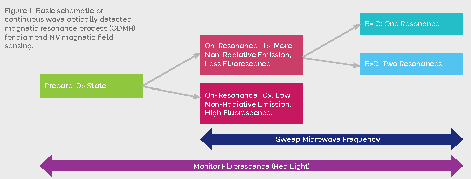
Fig. 1 — Basic schematic of continuous wave optically detected magnetic resonance process (ODMR) for diamond NV magnetic field sensing.
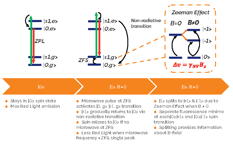
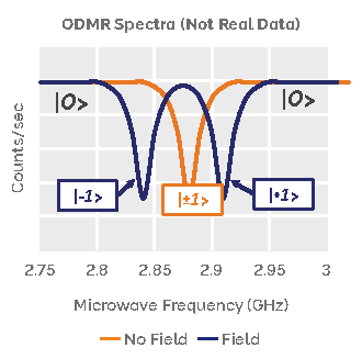
Fig. 2 — Schematic of Continuous Wave ODMR spin state transitions as a function of microwave frequency and B-field. The splitting between the |-1> and |+1> states depends on the magnitude and orientation of the applied magnetic field.
Colour centres are also potentially useful as optically addressable qubits. Coherence times can be extended through the use of cryogenic temperatures and isotopic purification for reduced 13C levels. The two-level qubit system can be defined as the |-1> and |+1> spin system and single qubit gates can be realised with microwave pulses on the order of the splitting. Two qubit gates can be realised with broader microwave pulses which interact with multiple qubits, akin to cross-resonance gates in superconducting qubit systems. Two qubit interactions are governed in part by the relative spacing between two defect qubits. Colour centre defects are of particular interest for future error-corrected and long-lasting quantum computing implementations. Their long coherence times may make these systems especially useful as quantum memories, whereby single photon states that must be held for a time during other computational steps could be transferred to a long-lived colour centre qubit until needed while other computational steps are carried out on, for instance, a photonic or superconducting quantum computing platform. The native microwave and optical connectivity of colour centre qubits offers multiple paths towards this future application, especially in conjunction with current efforts towards efficient state-preserving quantum transducers.
Device Fabrication Requirements and Challenges
The promise of colour centre quantum devices has motivated researchers to study, understand, and improve materials engineering for these systems. There are three key materials engineering needs for colour centres: (1) defect creation, (2) defect access, and (3) nanophotonic integration. Defect creation refers to challenges associated with the actual implantation and localisation of specified defects within a high quality host material.
Defect creation techniques often produce colour centre defects which are buried inconveniently deep within the host material. Many colour centre applications require defects to be closer to the surface in order to maximize the sensitivity of the colour centre to the environmental parameter of interest. In quantum magnetometry, the minimum magnetic dipole moment which can be detected, δμ, determines achievable device sensitivity. δμ scales as δμ ∝ r3 / √T2, where T2 is the spin coherence time and r is the distance between the NV centre and the target spin. This means that a defect 10 µm from a magnetic analyte has 1000x less sensitivity to that analyte than a defect which is only 1 µm away. Unfortunately, T2 of a colour centre defect is also quite sensitive to surface proximity, and not in a favorable direction.
Surfaces are no less problematic in colour centre quantum devices than they are in other quantum device modalities. T2 is notoriously sensitive to a range of surface-related decoherence sources, including dangling bond spins, crystal strain, trapped electric charges, surface adsorbates, shallow defects, and losses related to sub-optimal surface termination. Researchers have studied surface termination using hydrogen, oxygen, nitrogen, fluorine, and chlorine. The best results thus far have typically been found with an oxygen-terminated surface. Poor surface termination, with fluorine, for instance, can lead to bleaching and the consequent absence of an expected photon emission. Bleaching may occur because of a change in the charge state, which in the case of an NV(-) defect would change the defect to NV(0), perhaps induced by fluorine's increased electron affinity versus oxygen. Surface roughness is also a major contributor to poor T2 by increasing the density of surface-related decoherence sources. Colour centre applications require device fabrication processes which can improve access to deep defects by removing excess host material while maintaining a smooth surface and terminating dangling host material bonds with the preferred surface termination. This can be achieved with a multistep etch process developed at Oxford Instruments Plasma Technology which uses our PlasmaPro 100 Cobra ICP RIE.
The other key materials engineering challenge is nanophotonic integration. Even the most perfectly engineered colour centre must be integrated with other photonic structures in order to filter, guide and manipulate light. As an example, Sara Mouradian and colleagues in the Englund group fabricated crystalline photonic nanobeam cavities in diamond in order to improve the ZPL optical transition emission efficiency, which ordinarily is limited to only 3% due to phonon interactions. Their device fabrication exploited facet-dependent etch rates and both PECVD SiNx and ALD Al2O3 hardmasks as well as a series of ICP RIE etches to achieve depth-controlled undercut of the nanobeams in order to optimize the NV ZPL-active mode for high Q. These solutions can be achieved with the Oxford Instruments Plasma Technology PlasmaPro product line, which includes PECVD, ALD, and ICP RIE.
Paul Barclay's group at the University of Calgary's Institute for Quantum Science and Technology also works on diamond nanophotonic integration. As an example, they have recently published work on the development of high Q microdisk resonators to control NV centres with telecom wavelength light via a dual-transduction scheme utilizing optomechanical coupling between telecom band photons and microdisk phonon modes, followed by a stress coupling to the NV qubit spin. This scheme elegantly enables telecom band control without invoking additional optical transitions. Microdisk resonators function by coupling light from a nearby waveguide or optical fiber into a planar disk which is connected to the substrate only by a thin base. Constructive interference in the whispering gallery mode of the resonator creates radiation pressure which excites mechanical vibrations in the device. If the device is engineered such that the dominant mechanical mode is a swelling of the device (a momentary change in the effective diameter of the disk – known as a breathing mode) and appropriate colour centres are implanted into the microdisk, the induced mechanical strain interacts with NV qubit spins. The Barclay group has utilized similar microdisk resonators to accomplish low-noise phonon-mediated transduction in diamond between a range of photon wavelengths with more conventional photon-phonon-photon coupling schemes. As with Mouradian et. al.'s nanobeams, the Barclay group's microdisk resonators require sophisticated multi-layer fabrication with hardmasks, anisotropic etch processes, and isotropic undercut etches in order to achieve the intended design with high quality factor. This type of process is considered a "quasi-isotropic" process and was recently used at Stanford to fabricate one-dimensional photonic crystal resonators for significant enhancement of emission from SnV(-) colour centres. Diamond etching has also been used at TU Delft for fabrication of Fabry-Perot microcavities for quantum networks. Oxford Instruments Plasma Technology's PlasmaPro 100 Cobra ICP RIE provides the control needed to successfully manufacture these sensitive devices.
A range of other photonic structures are also under investigation for use in colour centre manipulation and control in both diamond and SiC host materials. These structures include passive components required for light routing and coupling, such as low-loss waveguides, cavity photonics, and grating couplers, as well as active components such as interferometers and waveguide-integrated superconducting nanowire single photon detectors (SNSPD). Smooth etches are extremely important in order to avoid waveguide loss, which scales as σ2/λ3, where σ is rms roughness. Superconducting nitride ALD is promising for integrated in-plane SNSPDs, which often use thin superconducting nitrides. Oxford Instruments Plasma Technology's FlexAL® ALD's unique combination of plasma enhanced ALD and driven lower electrode has been used to make high performance NbN-based SNSPDs.
Oxford Instruments Plasma Technology Etch Solutions for Colour Centre Devices
Oxford Instruments Plasma Technology has years of experience developing processes for both diamond and SiC etch. While our earliest experience with these materials focused on other applications – diamond scalpel blades and power devices – we have been very successful in expanding and adapting our expertise for our customers in the quantum device space. Both of these colour centre platforms require extremely high-quality processes for thinning in order to increase colour centre access while maintaining and even improving the surface quality for optimal T2.
Our process was developed in collaboration with other UK partners for a fast diamond etch with an accurate and controllable stop 2 µm from the NV centres. This etch is needed to remove damage and contamination from the as-received substrate surface, and reduce roughness as much as possible to avoid photon scattering losses and noise at the diamond-air interface. The etched surface then needs to be left in an O-terminated state. This process was to be maskless and needed to quickly remove many microns of material in order to increase access to the deeply-implanted NV centres. We studied two etch chemistries using our PlasmaPro 100 Cobra ICP RIE, which features a high ion density ICP source and is capable of processing wafer sizes up to 200 mm – an isotropic O2 etch and an anisotropic Ar-Cl2 process. While the O2 etch was fast and left the surface relatively smooth and in the preferred O-terminated state, we found that the process left the surface with some degree of pitting irrespective of etch parameters due to the inability of O2 to remove inorganic surface contaminants. The Cl2-based process was also fast and was quite effective in removing surface contaminants, but slightly increased roughness (by 0.8 Å from a starting roughness of 2.05 Å) and did not leave the surface in the preferred O-terminated state. Ultimately, we found that the ideal process was a multi-step combination of the two etches, wherein the Ar-Cl2 etch was tuned to remove initial surface contamination and etch the bulk of the material at a rate exceeding 100 nm/min, and the O2 etch was used as a finishing step to ensure a smooth and O-terminated final surface for maximum T2. We also studied the selectivity of these etch processes to a quartz mask and found that the O2 etch was far more selective, at approximately a 300:1 selectivity versus the 1:1 selectivity of the more physical bulk Ar-Cl2 etch. AFM showed a final post-etch Ra roughness below 3 Å, as measured on an Oxford Instruments Asylum Research Jupiter XR AFM. Atomic Layer Etch (ALE) is also available as an option on the PlasmaPro 100 Cobra ICP RIE and can be used as a finishing step to an etch process. While a relatively new technology, ALE has already been used to etch carbon and may be well-suited for etches within tens of nm of colour centres, where spin coherence is especially sensitive to disorder at the diamond surface.
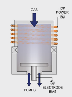
Fig. 3 — Schematic of Oxford Instruments PlasmaPro 100 ICP RIE.
Oxford Instruments' PlasmaPro 100 Cobra ICP RIE platform is also well-suited for patterned diamond etch. Many of the finest etches on this platform have been developed by the aforementioned Barclay group, which has developed a process to create sophisticated undercut microdisk resonator structures in diamond. Their process starts with a diamond substrate coated by a layer of PECVD Si3N4 underneath patterned Electron Beam Lithography (EBL) resist. The EBL pattern is transferred to the Si3N4 hardmask by a C4F8-SF6 ICP RIE etch and further transferred to the desired depth in diamond by an O2 etch, for which etch anisotropy is induced by electrode bias within the etch chamber. A second conformal layer of Si3N4 is then deposited to protect the sidewalls of the disk portion of the microdisk resonator and maintain the distance from the disk edges to the rest of the substrate. The microdisk is then undercut by an isotropic O2 etch. The isotropic nature of the etch is controlled by the application of low- or zero-bias during the etch, ensuring that oxygen ion directionality is minimized. The crystal planes of the diamond influence the precise geometry of the undercut. These processes were developed using Oxford Instruments Plasma Technology's range of advanced PlasmaPro 100 device fabrication tools.
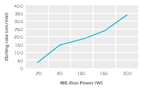
Fig. 4 — Example of etch rate vs bias power for ICP RIE diamond etch process.
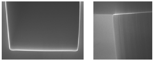
Figure 5. SiC etch results. Cross‑sections of SiC after anisotropic etch with Oxford Instruments Polaris ICP RIE.
We have also demonstrated excellent results for SiC etch. Patterned etches are realised in SiC up to moderate depth (10 – 20 µm) with the use of hardmask materials such as SiO2 and Al, or very thick mask materials such as SU-8. Deeper etches are possible with a Ni hardmask. We anticipate increasing need for sophisticated SiC processing for colour centre applications as the field matures and grows, both because of its unique suitability for NIR sensor applications, and because of the preference for SiC's larger available wafer sizes (100 – 150 mm) and overall greater maturity of device fabrication on the SiC platform in industry.
Conclusions
There is tremendous opportunity in the field of colour centre-based quantum devices. Diamond NV centres have already found applications in sensing, but many more applications will be possible only with further development and discovery of optimal host-defect systems and of device fabrication requirements and processes. While we have focused primarily on the promising diamond and SiC host materials in this whitepaper, Oxford Instruments Plasma Technology also has extensive experience with a wide range of other materials which are being explored for use in colour centre applications, including hexagonal boron nitride, TiO2, Si, ZnO, MoS2, and many more. We are committed to supporting quantum device research globally, as demonstrated by the processes we are developing, the collaborators and partners we are supporting, and the consortia and working groups we are engaged with in this space.
Acknowledgements
The author would like to acknowledge Dr. Sara Mouradian for helpful discussions.

