Introduction
Reactive Ion Beam Etching (RIBE) is a technique well suited to etching slanted features. The technique allows localised removal of material using a broad ion beam. The material is removed at the wafer surface following collisions between accelerated ions and reactive species formed in the ion source. Control and repeatability in defining slanted features is contingent on advanced ion beam source configuration and experienced selection of processing conditions.
In this paper, we describe how Oxford Instruments Plasma Technology solution delivers controlled processing of slanted gratings used as light couplers for Augmented Reality waveguide combiners. We demonstrate control of the slant angle, the groove depth and the filling ratio for large wafer sizes.
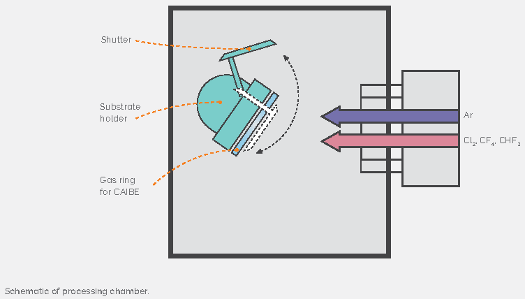
Fig. 1 — Schematic of ion beam processing chamber. The wafer is positioned on a substrate holder which is angled to face the ion source. The angle of the substrate holder can be adjusted to enable angled etching.
High Uniformity of the Etching Depth at Slanted Angles
Plasma Technology solution for uniform etching is based on RIBE etching of an angled substrate. Figure 1 illustrates typical processing conditions. Control of the slant angle is enabled by Plasma Technology's custom made highly directional ion beam combined with an adjustable substrate holder tilt controlled to 0. Currently, the slanting angle is controlled from 35° to 60°. When etching slanted features, the angled position of the substrate causes non-uniformity of the etch depth which becomes more difficult to control without rotating the substrate.
To achieve uniform etching over a large area, our proprietary hardware design compensates for non-uniformity in the ion flux. This design allows for optimization of the local etch uniformity over a range of angles. To demonstrate a large processing area with excellent uniformity, a 200 mm SiO2 on Si wafer was etched. The results demonstrate an excellent uniformity for slant angles ranging from 35° to 55° deg. The graph below shows full wafer data for grating angles 35°, 45° and 55°.

Fig. 2 — Etching depth map across 200 mm wafer size, demonstrating excellent uniformity for slant angles ranging from 35° to 55°.
Maintaining the Filling Ratio with Uniform and Parallel Features
The filling ratio depends on the Critical Dimension (CD) which must be controlled at every step of the manufacturing process. As the features are transferred from multiple masks to the final substrate, an accurate understanding of the CD variation at each step will allow manufacturers to control the CD on the final substrate.
The profile of each sidewall Φ1 and Φ2 must be controlled to define both the overall slant profile and the parallelism of the features. This allows the filling ratio to be maintained throughout the etching process.
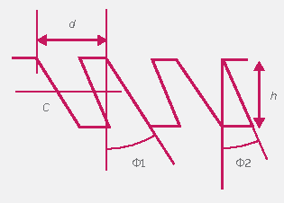
Fig. 3 — Schematic of slanted grating with critical parameters highlighted: filling ratio c/d, the depth h and the slant profile Φ for each sidewall.
The RIBE technique is well suited to manufacturing gratings as it allows for minimal variation of the CD, hence filling ratio. The relatively low ion density compared to conventional ICP etching makes it a less reactive technique. Glass and quartz can be etched using similar techniques, although careful processing is required to address impurities present in the glass. Plasma Technology's solutions use Fluorine based chemistry for enhanced CD control performance on both materials. When using a Cr mask, this chemistry leads to the formation of CrFx which protects the mask, as it is non-volatile under the processing conditions. The CrFx by-products thus provide high selectivity Quartz/Glass, whilst limiting the lateral etch rate of the mask, and thus provides control over the CD variation.
In particular, when etching at an angle, the position of the substrate can generate ion deflections as well as ion shadowing which will often introduce non-parallelism of the features in the grating. One example is shown on Figure 4. This phenomenon tends to be amplified when operating at high ion energy, i.e. higher etch rate. To minimise this effect, Plasma Technology's low temperature plasma produces slow (cold) ions (ion temperatures <1eV) which are extracted from the ion source via grids with a well-defined energy. The beam parameters are also adjusted with a careful choice of gas mixture and ratio. The amount of reactive gas is balanced to keep the groove fully open with a clear square base. For a given angle, the accuracy is typically below ±2° deg and parallelism Φ1 and Φ2 is less than ±5° deg over 200 mm area.
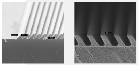
Fig. 4 — SEM cross section of slanted grating. (left) Process non-optimized showing non-parallel sidewalls with limited control of the base profile. (right) Fully optimized process results showing high parallelism between sidewalls.
Hard Mask Processing
A critical process to master in order to gain control of the CD is the mask opening step. Chromium (Cr) is commonly used as a mask and etched using Inductively Coupled Plasma (ICP) etching. The process uses a mixture of Chlorine and Oxygen to form CrClxOy which is volatile under the processing conditions. Both gases are necessary when etching Cr since CrClx and Cr2O3 are both non-volatile under the processing conditions. Boiling temperatures are given in the table below.
| By-product | Boiling temperature (°C) |
| CrClx (x = 1–3) | 1152 |
| Cr2O3 | 2435 |
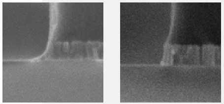
Fig. 5 — Boiling temperature for Cr etching by-products.
Since Cr etches chemically, and therefore requires little ion energy to etch, it tends to etch isotropically which translates as a variation of the CD. As the CD variation can be compensated by the lithography, it is best to guarantee a uniform CD variation across the substrate rather than minimal CD variation. This variation can be limited by controlling the gas ratio and gas distribution in the processing chamber.
Additionally, a foot is often observed on the Cr profile which contributes to the CD variation. A foot will also very likely introduce irregularities on the sidewalls of the final Quartz/Silicon groove, since it will etch away quicker as it is thinner. In order to maintain the CD of the grating, it is therefore critical to keep the foot to a minimum. Depending on the size of the features, it is possible to remove the foot by increasing the ion energy to sputter the excess foot. However, increasing the ion energy can be limited in order to achieve sufficient selectivity to the resist mask. An alternative is to over-etch the features. During the over-etch, the process tends to etch sideways because of the high selectivity to the underlying substrate. The over-etch can be controlled by using an end-point detection system. Both laser and optical emission spectroscopy are suitable for this type of application. However, considering the small exposed area often used for diffractive gratings for AR, the laser end-point system is often more reliable.
Achieving a vertical profile with minimum footing is critical to demonstrate excellent CD control.
Conclusion
Plasma Technology unique ion beam technology has been applied to deliver a solution for manufacturing slanted features. The solution was demonstrated on challenging slanted grating for Augmented Reality where manufacturing tolerances are very strict. Excellent uniformity of the etching depth is demonstrated on large 200 mm wafer size at multiple slanted angles. Key process control for both masking and etching are also identified to demonstrate control of the slanting angle below ±2° with excellent parallelism.

