Introduction
The properties of InP which combine a wide band gap with high electron mobility, make it a desirable semiconductor for the manufacture of optoelectronic devices. A key application is communication and this is expanding rapidly with increased data traffic.
InP enables the manufacture of components that can operate at high frequencies allowing higher volumes of data. In particular it offers compelling advantages for laser diode manufacture delivering excellent functionality at a competitive price. When design and fabrication is optimised InP lasers provide high spectral purity and optical power, over a wide temperature range. Furthermore the achievable wavelength range of 1100 – 2000nm is optimal for fibre optic communications. Establishing cost-effective processing strategies for the production of InP lasers therefore directly supports the advancement of communications to support the ever increasing demand for data transfer.
In this white paper we examine the role of plasma processing technologies in InP laser diode manufacture focusing on the relative merits of inductively coupled plasma chemical vapour deposition (ICPCVD) and plasma enhanced CVD (PECVD). A primary aim is to highlight the relevant characteristics of different processes and show how they can be optimally applied, in combination, to efficiently fabricate high performance lasers.
Introducing the Core Plasma Processing Technologies for InP Laser Fabrication
Plasma can be described as a fourth state of matter containing positive ions, electrons, radicals and non-ionised gas. Ionising a gas requires the input of significant amounts of energy (usually electrical or thermal) and the resulting plasma is highly energetic with properties which are well suited for well controlled semiconductor manufacture. These properties can be tuned through the manipulation of chemistry, by varying plasma composition or processing conditions such as pressure or wafer temperature offering exceptional flexibility to achieve and precisely control a very wide range of surface interactions. Furthermore because they contain free electrons, plasmas can be controlled both by electrical and/or magnetic fields within processing equipment. These inherent attractions have led to the commercialisation of highly productive and configurable plasma-based process tools for semiconductor device fabrication. Those utilising the following techniques are particularly valuable for InP laser fabrication:
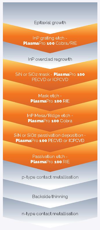
Fig. 1 — The processing steps involved in the fabrication of an InP laser with those implemented using plasma processing methods highlighted in orange
PECVD – Desirable Film Properties for a Wide Range of Materials
PECVD involves the reaction and deposition of ionised gases from a plasma onto a substrate to form a film or coating.
Figure 1 shows the key features of a PECVD system. A gas mixture is pumped into the vacuum chamber via a "showerhead" gas inlet in the top electrode and plasma is generated by the application of RF power. Deposition occurs on the substrate surface as radicals and ions from the plasma form material on the sample, with unused material pumped away. Operating pressures are typically in the region of 0.5 to 1.0 Torr.
PECVD can be used for an extremely wide range of materials, including SiOx and SiNx both of which are used for masking subsequent etch processes or passivation deposition in InP fabrication. It produces uniform high quality films, more specifically high density films with minimal pinholing, and enables the close control of material properties such as refractive index and hardness. Operating temperatures for PECVD processes typically lie in the range 90 – 650°C with substrate temperatures ~300°C used for processing InP.
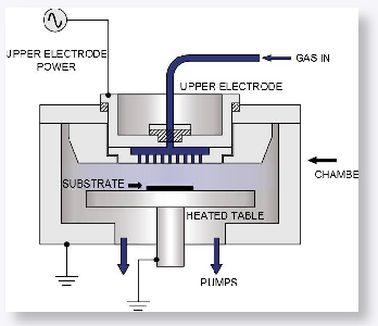
Fig. 2 — PECVD enables the deposition of high quality films at relatively low working temperatures
ICPCVD – Plasma Deposition at Low Temperatures with Minimal Substrate Damage
In ICPCVD, as the name suggests, an ICP is used in place of the electrically generated plasma applied in PECVD processes. Inert gases are fed in at the top of the vacuum chamber and converted to plasma as they pass through the powered coil. A second gas feed point just above the substrate enables the separate introduction of reactant gases which trigger the formation of the film, along with dopants where required. RF biasing can be applied across the substrate table to manipulate the properties of the film. Operating pressures are typically in the region of 1 – 10 mtorr, far lower than for PECVD.
ICP results in a high density flux at the substrate surface. This enables the production of high quality films at lower temperatures than those achievable with PECVD. Operating temperatures for ICPCVD processes are typically in the range 20 – 400°C, though higher temperatures are accessible with the substrate typically maintained at a temperature of ~150°C or less. This is an important advantage, particularly for certain Si-based materials. ICPCVD is also associated with low substrate damage. This is attributable to the low ion energies associated with deposition and/or the remoteness of the plasma. Generally speaking ICPCVD provides excellent coverage and is prized for delivering good conformality, particularly for deeper features.
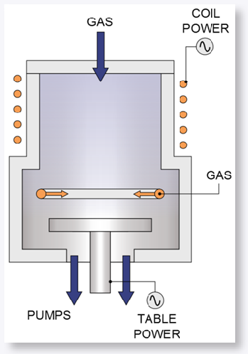
Fig. 3 — ICPCVD enables low temperature deposition with minimal substrate damage
Choosing an Optimal Processing Technology for Each Fabrication Step
An understanding of the different features of alternative plasma processing techniques aids assessment of their relevance and suitability for different stages of the InP fabrication process. Figure 1 shows the steps involved in the construction of a typical InP laser, highlighting the plasma processing techniques that are most suitable for each. While each step is important it is the InP Mesa/Ridge etch that is arguably most critical with the properties of the resulting waveguide having a defining impact on the quality of the finished laser. In the following sections we consider the selection of plasma processes for each step, with reference to example performance data. These data are derived from experience with Oxford Instruments systems in each specific application, either in laboratory and/or proof of performance studies or within the manufacturing environment.
Fabricating the InP Mesa/Ridge Mask
The choice of material for the InP Mesa/Ridge mask typically lies between SiNx and SiOx. SiNx has a tendency to facet less resulting in a good right-angled profile with less pronounced rounding than is observed with SiOx and is often the preference. Faceting is where the top corners of a masking pattern are eroded faster than the planar surfaces and can compromise mask quality. In either case the mask is patterned using photoresist, which is then removed prior to etching of the InP through the SiNx/SiOx. Residual mask is subsequently removed in a final step.
Choice of technique for mask deposition is usually based primarily on film quality, though deposition rate is also important. High film quality, more specifically high film density, is associated with high selectivity during the subsequent etch and is quantified for comparative purposes via wet etch rates (WERs), measured under standardised conditions using potassium hydroxide or buffered HF (buffered oxide etch – BOE).
A further consideration is the need for hydrogen-free deposition. In certain circumstances hydrogen can change the stoichiometry of InP during processing, thereby influencing the performance of the device. Removing any possibility of hydrogen evolution by avoiding the use of ammonia for example as a deposition gas is common practice.
Table 1 contrasts the operating conditions for PECVD and ICPCVD, the alternative processes for mask deposition. PECVD is the faster process and usually the preference except in applications where there is a temperature limitation. Here the lower operating temperature of ICPCVD is an advantage that more than offsets the somewhat lower deposition rates obtained. Both PECVD and ICPCVD can be deployed with low hydrogen process chemistries where required.
| PECVD | ICPCVD |
| Recommended temperature range | 90°C – 650°C | 20°C – 400°C (higher temperatures possible) |
| Equivalent temperature | ~300°C | ~100°C |
| Stress control methods | SiNx – LF power, He addition, power pressure SiOx – SiH4 power | All film types, process conditions, e.g. ICP power, pressure |
| Process pressures | 600 – 3000m Torr | 2 – 30m Torr |
| Power ranges | 20 – 1000W | 150W – 2000W |
| Deposition rates | 7 – 1200nm/min | 6 – 150nm/min |
Table 1: PECVD delivers high SiNx/SiOx deposition rates but requires higher operating temperatures which can be a limitation for some devices
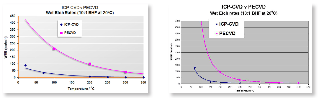
Fig. 4 — Wet etch rates highlight the higher quality of SiNx films (upper graph), relative to SiOx analogues (lower graph), and the ability of ICPCVD to deliver high quality films at low processing temperatures
Figure 4 compares WERs for both SiNx and SiOx films made by PECVD and ICPCVD. In terms of film quality the SiNx films are superior to those fabricated from SiOx, regardless of processing technique. However, the films deposited by ICPCVD are superior to those deposited by PECVD as well as exhibiting performance that is less temperature dependent. In all cases film quality improves with processing temperature but this effect is particularly modest with ICPCVD SiNx films, which exhibit excellent quality when manufactured at very low temperatures.
RIE is typically used for etching of this mask as it offers a simple cost effective option for this relatively undemanding application, where etch rates tend are not critical. Figure 5 shows the results of using RIE to etch a SiN mask. This etch was carried out using a SF6-CHF3 process using a PlasmaPro 100 RIE. An excellent vertical feature was achieved; this is essential to create a vertical InP profile during the following etch step.
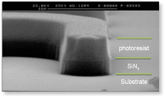
Fig. 5 — RIE can be used, along with photoresist, to fabricate a high quality SiNx mask for etching of the InP Mesa/Ridge
Passivation Deposition
The final plasma processing step in InP laser fabrication is the deposition of a passivation layer and associated etching to enable electrical contacts to be implemented as required. SiNx or SiOx are again the materials of choice and this step has much in common with the preceding mask deposition. The technology choice typically comes down to PECVD or ICPCVD with the latter preferred for temperature sensitive applications. Film quality at this point in this process is directly associated with protection of the device, with higher density films resisting the ingress of water more effectively and enabling the application of higher voltages prior to breakdown.
In Conclusion
Fabrication of the waveguides and gratings that deliver desirable performance in an InP laser diode requires the considered use of a range of plasma processing techniques. A suite of powerful and flexible plasma processing tools enable laser manufacturers to efficiently apply these techniques to achieve the deposition, masking and etching that is essential for the precise control of feature characteristics. A basic understanding of the strengths and limitations of these tools helps manufacturers to consistently produce the precisely controlled, smooth vertical profiles associated with exemplary device performance while simultaneously maximising throughput and minimising the cost of production.

