Introduction
Semiconductor technology is becoming increasingly important in global healthcare enabling novel understanding, discovery and treatment of disease to make healthcare more affordable and efficient, both in and out of the clinic.
With the global healthcare industry being valued at US $1.65 trillion in 2016 and expected to reach US $2.69 trillion by 2025, it is an important growing industry. Key drivers behind this ongoing market growth are growing and aging populations, over urbanization, rising disease prevalence all of which are putting further strain on our healthcare systems which are already grappling with issues relating to access, quality, and cost. Convergence of technology from the seemingly disparate fields of semiconductor device processing, life sciences are fast revolutionising healthcare and medical research by enabling quick and accurate diagnosis. This in turn is increasing the speed and efficiency of treatment for various conditions as well as biomedical research and development.
Biomedical Device Processing
Biomedical devices are a class of miniaturized electronic devices that are assembled by integration of microfluidics, active sensors/transducers and the supporting signal processing electronics.
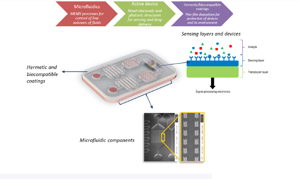
Fig. 1 — Major processing requirements for biomedical device fabrication
The similarity of fabrication techniques for this class of devices to those of microelectronics not only allows researchers and engineers to leverage decades of microelectronics processing experience but also provides a rapid route to scale up for new technologies. The very first integrated devices were fabricated on silicon (Si) substrates followed by glass (SiO2) which brought some advantages. Today's devices are hybrids that combine glass, silicon and various polymers like acrylic, resists, thermoplastics and several other novel nano-electronic and photonic materials. Semiconductor fabrication techniques provide the required economies of scale to make this technology cost effective, maintaining precision and continued miniaturization and creating devices that remain functional over long term use.
This white paper is the first of four aimed at giving an overview of various semiconductor processing technologies, their advantages and challenges for fabrication of such biomedical devices. This edition is focussed on dry processing solutions for fabrication of microfluidic components.
Microfluidics
Microfluidics is a powerful technology that allows the flow and control of tiny amounts of fluids. It has enabled miniaturization of analytic setups used in larger fluidic structures. These structures perform functions such as analyte transport, purification, separation, reaction, immobilization as well as pathogen or disease biomarker detection. Advances in Micro-Electro-Mechanical-Systems (MEMS) manufacturing techniques allow reliable and uniform fabrication of devices that can move fluids with volumes down to picolitres into active regions of the device. This is enabling powerful devices for next generation sequencing, drug discovery, delivery, bioanalysis, point of care diagnostics and several other tools for life science research.
Microfluidic components range from passive components such as channels and wells used primarily for reagent or analyte manipulations to active ones such as jets, meshes and nozzles which are integrated to form complete functional chips. Materials selected for a particular device direct the manufacturing technique, performance, functionality, and the cost of the device. Typical microfluidics devices are manufactured with material such as glass, silicon, and polymers (plastics and photoresists).
Glass has traditionally been employed as the preferred material because of its well-understood physical, chemical, and thermal properties. It lends itself well to applications that require optical transparency, a low fluorescence background and a low channel surface roughness such as micro capillary electrophoresis (μCE) devices and fluorescence-based identification of cells, DNA or other biomarkers flowing in the micro-channels. Silicon is favoured for the ability to achieve high-aspect ratio micro/nano structures and multifunctional heterostructures. This is often used in conjunction with glass to allow transparent windows into the flow channels as deep vertical channels can be fabricated using well known semiconductor processes, which means larger areas are available on the surface to enable stronger bonding and allow higher pressure microfluidics. Polymers also provide significant advantages where optical transparency and low thermal expansion are not critical factors and here silicon-based MEMS structures are micro-fabricated as small feature size moulds to create polymer replicas.
Fabrication of Microfluidic Devices
Vertical etch profiles and high aspect ratios are often required for microfluidic devices. This precludes the use of wet chemical etching which is isotropic. Therefore dry etching techniques using plasma are mainly employed. Depending on the application several different approaches and materials choices exist for the fabrication of active and passive microfluidic devices. Oxford Instruments offer several solutions for the fabrication of MEMS structures for such devices from small coupons for R&D all the way up to 200 mm uniform processing for production applications. With over 30 years of experience in semiconductor processing, Oxford Instruments has been at the forefront of MEMS process development using plasma enhanced etching and deposition processes. Plasma enhanced etching ideally suited for applications such as microfluidics and other biological MEMS structures where control over feature morphology is critical. This can be achieved by variation of plasma chemistry, composition and other process parameters such as wafer temperature and process pressure. Inductively Coupled Plasma Reactive Ion Etching (ICP RIE) using fluorine-based chemistry is a widely used technique for etching deep structures in silicon and glass. Such plasma etching exploits both chemical and physical processes to volatilize and remove solid material.
The Deep Silicon Etch Process: A Work Horse for a Wide Variety of Microfluidic Applications
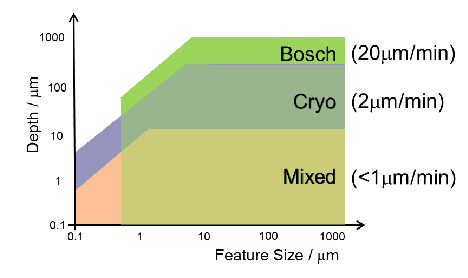
Etching of silicon is done using a plasma flux containing fluorine species onto the surface and the choice of the recommended process is strongly dependant on the application as summarized in Figure 2. In general:
- Bosch process: This is typically used for features >1µm and depths >10µm and uses quick switching between pulses of SF6 and C4F8 to alternately etch and passivate the walls with a polymer which enables high etch rates, selectivity and anisotropy.
- Cryogenic Deep Silicon Etch (Cryo-DSiE): This process uses fluorine radicals to etch silicon. However, instead of using a fluorocarbon polymer, this process relies on forming a blocking layer of oxide/fluoride (SiOxFy) on the sidewalls (around 10–20nm thick) at cryogenic temperatures inhibiting attack by the fluorine radicals. Cryo-DSiE is typically used for smooth sidewalls and/or nano-etching or tapered profiles in applications such as micro moulds etc.
- Mixed processes where SF6 is mixed in the same step with C4F8 or use HBr based chemistry (for example for very high selectivity over SiO2) are also an option for shallow, low aspect fine features.
The choice of process is a balancing act between speed and control and is very application dependant. For example, the traditional Bosch process is widely used for fast anisotropic etching applications while the Cryo process delivers its advantage where feature sizes are in nano-scale, smooth side walls are critical and rate is not a major concern.
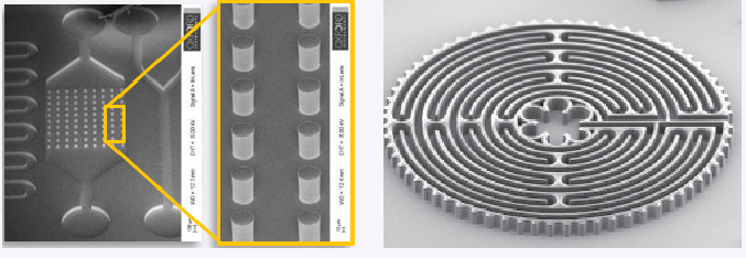
Fig. 2 — Choice of the deep silicon etch depends on the rate and depth of features required
| Parameter | Bosch | Cryo | Mixed Gas |
| Rate | High | Moderate | Low |
| Selectivity to PR | Very High | High | Low |
| Profile | Vertical | Vertical or sloped | Vertical or sloped |
| Aspect ratio | Very High | High | Low |
| Sidewalls | Scallops | Smooth | Smooth |
| ARDE control | Yes | Limited | Limited |
| Cleaning | Infrequent | Rare | Regular |
| Min. feature/nm | ~300 | ~10 | ~30 |
Glass and Deep Oxide Etching
Etching of glass requires high ion energies. This is due to the energies required to break the strong Si-O bonds and to remove any impurities which are present in the various grades of glass. Therefore glass etching typically occurs at lower rates compared to silicon and the etching shows lower selectivities. This process can produce "fences" which are caused by incomplete removal of sidewall polymer after etching. Oxford Instruments glass etch solutions control this problem via process and hardware optimizations to provide extremely stable and repeated rate and selectivity with excellent sidewalls control and zero fencing.
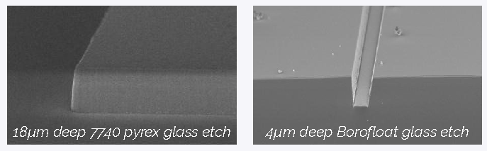
Fig. 3 — Glass etching on Oxford Instruments process modules: 18µm deep 7740 pyrex glass etch and 4µm deep Borofloat glass etch
Etching of Polymers
Point-of-care (POC) diagnostic applications often have very stringent demands on cost. Polymers offer an effective alternative to materials like silicon and glass in this respect. There are several material options again depending on the demands of the application and most commonly used ones for microfluidic channels nowadays are SU8, polyimide (PI), PDMS (poly-dimethyl siloxane), PMMA (poly-methylmethacrylate) and COP (cyclic olefin copolymer). For example, materials like PDMS and PMMA are not chemically resistant against many industrial solvents used in a semiconductor cleanroom which is an issue when integration of microfluidics with the signal processing electronics or the sensing elements is required for POC devices. Oxford Instruments has expertise in etching SU-8 and polyimide films using plasma etching techniques.
SU-8 is an epoxy based photoresist that has been used extensively for making high aspect ratio MEMS device structures because of good mechanical properties, water impermeability, dielectric nature and compatibility with semiconductor fabrication. It is also bio-compatible and resistant to chemicals which makes it ideally suited to the fabrication of micro channels for microfluidics and bioMEMS devices. While a simple oxygen plasma etch is sufficient for etching most solid photoresists, adding fluorinated species can significantly enhance etch rates but can lead to a loss in uniformity and selectivity. Careful optimisation of the process parameters is needed in that case and excellent uniformity can be maintained.
Polyimide (PI) is an emerging candidate material for microfluidics based devices. In addition to its biocompatibility and chemical resistance, the high glass-transition temperature of around 325°C enables PI to withstand most processing steps. Like SU-8, PI can also be etched using O2 (with CF4/SF6 in case of silicon additives in PI) using Oxford Instruments RIE or ICP RIE solutions.
Conclusion
Advancement in fabrication technology for microfluidics over the years has facilitated applications in the biomedical industry and accelerated R&D in the life sciences. Plasma based process solutions form a critical tool for the fabrication of microfluidics with control and precision while enabling the flexibility of design for various applications. The range of plasma processing techniques offered by Oxford Instruments allows researchers and device manufacturers to work with multiple material platforms (Silicon, Glass, Polymer etc) and have full control over the properties of microfluidic features.
Next Time
A key requirement of microfluidics fabrication for biomedical devices is the ability to control surface properties after the creation of channels. In the next white paper we will overview processing solutions for hydrophobic and hydrophilic surface creation which is critical for both active functions of the device as well as for post processing challenges such as bonding, sealing and de-scum.

