Introduction
Semiconductor technology is becoming increasingly important in global healthcare; enabling novel understanding, discovery and treatment of disease to make healthcare more affordable and efficient, both in and out of the clinic. With the global healthcare industry being valued at US $1.65 trillion in 2016 and expected to reach US $2.69 trillion by 2025, it is an important growing industry. Key drivers behind this ongoing market growth are growing and ageing populations, over urbanization and rising disease prevalence. All of which are putting further strain on our healthcare systems which are already grappling with issues relating to access, quality, and cost. Convergence of technology from the seemingly disparate fields of semiconductor device processing and life sciences are fast revolutionising healthcare and medical research by enabling quick and accurate diagnosis. This in turn is increasing the speed and efficiency of treatment for various conditions as well as biomedical research and development.
Previously…
In the previous editions of this white paper series we delved into the various aspects of plasma processing techniques, from microfluidic channel creation and surface wettability control to creation of active electronic, photonic and MEMS devices for biomedical applications. These processes outline the breadth of Oxford Instruments’ process capabilities to design and tailor devices based on the requirements of wide variety of end applications.
Barrier and Biocompatible Coatings
Biomedical devices require a wide range of thin film coatings which serve as layers for surface protection and passivation; rendering the device biocompatible. Depending on the device architecture, barrier layers are almost always required which protect the device from failures that can be broadly classified as follows:
- Component failure: Relevant for both in-vitro and in-vivo applications this type of failure occurs due to effects such as electrical shorts or response drifts due to penetration of analytes or liquid environment. Here, layers that protect the device from moisture and liquids by acting as barrier layers.
- Biocompatibility failure: Critical during in-vivo applications, this type of failure could occur due to effects such as biofouling where cellular matter adsorbs on the active surface thereby impeding analyte diffusion at the biosensor surface, ultimately leading to a decrease in sensor response.

Fig. 1 — Major processing requirements for biomedical device fabrication
In addition to device failures, it is vital to consider hermeticity and biocompatibility of the device itself to ensure that there is no diffusion of possible toxic materials out of the device into the body (thus minimize body reaction) and no diffusion of liquids or moisture back into the device.
Various thin-film approaches have been investigated for barrier coatings on medical devices. Thin film technology provides the advantage of maintaining small sizes of devices compared to conventional methods. Such films are usually deposited by vapour deposition techniques such as CVD, PECVD and ICPCVD which are widely used for deposition of silicon oxides, silicon nitrides or aluminium oxides as barrier materials. More recent efforts are directed towards utilizing Atomic Layer Deposition (ALD) as barrier layers. The ability of ALD to deposit ultra-thin yet high density conformal layers that covers every corner of the device makes it a very attractive technique for such applications. ALD processes commonly use two volatile precursors which are sequentially introduced into the reactor chamber, and this cycle is repeated until the desired coating thickness is achieved. State of the art research and development efforts are directed towards nanolaminates of inorganic and organic layers to combine the flexibility and mechanical properties of organic materials like parylene and polyimides with extremely thin and biocompatible layers like Al2O3, HfO2 and TiO2 that form excellent diffusion barriers.
Oxford Instruments plasma enhanced barrier layer deposition solutions provide the advantage of deposition of high-quality films at low temperatures. For example TiO2, which is a commonly used biocompatible material, generally needs plasma activation for deposition at low temperatures. These layers can provide protection and biocompatibility both against moisture as well as in liquids:
- SiNx and Al2O3/HfO2 layers have commonly been used as moisture protection layers. These are measured using water vapour transmission rate (WVTR) experiments. PEALD Al2O3 layers deposited at room temperature functions as an excellent single layer barrier with WVTR = ≤ 2·10-6 g·m-2·day-1. Laminates of Al2O3 with other layers such as TiO2, SiOx, HfOx and Alucones can further improve the properties of the barrier layer stack by reducing defect numbers (by avoiding formation of pinholes) and improving flexibility and improve corrosion resistance.
- ALD Al2O3/HfO2 films also function as dielectric protective layers for biosensing devices working in vitro. Insulating layers of amorphous alumina deposited by plasma enhanced atomic layer deposition (PEALD) using pulses of TMA and Oxygen plasma at low temperatures have been shown to be successful in protecting the SOI nanowire FET based biosensors, while detecting bovine serum albumin (BSA) with femto-molar sensitivity in liquid for periods up to half a year.
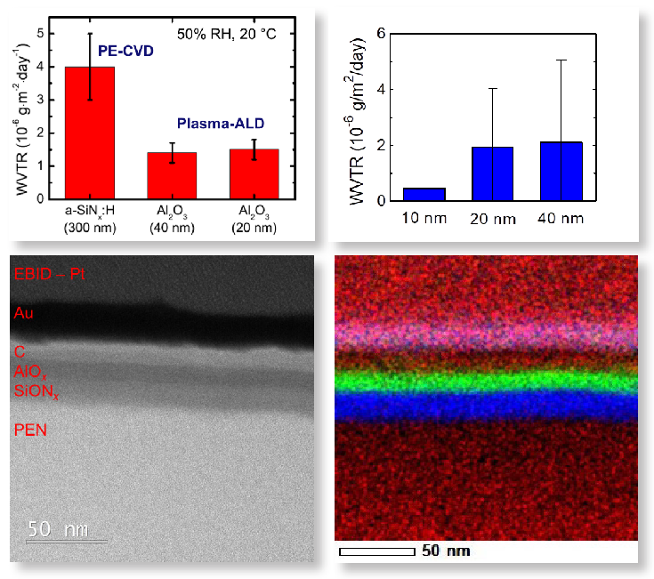
Fig. 2 — (a) WVTR of SiN x and Al
2
O
3 barrier layers deposited by PECVD and PEALD respectively; (b) WVTR of PE-ALD SiN x ; (c,d) A barrier layer stack of SiN x and AlO x deposited on polyethylene naphthalate.
Conclusion
Barrier coatings play a critical role in ensuring reliable and efficient function of biomedical devices for long periods of time in complex biochemical environments. These not only serve as barrier layers for active devices in harsh environments but also protect sensitive analytes from effects such as fouling due to the toxicity of some of the layers. Atomic layer deposition has become the standard for the fabrication of such layers. Coatings via this technique are conformal, extremely dense and pin-hole free with atomic level thickness control, which enables extremely good encapsulation on complex device surfaces. Oxford Instruments’ Plasma Enhanced ALD (PEALD) solutions enable deposition of these critical layers with high quality while processing at stringent temperature limits posed by these applications.
References
- Nehm et al., ACS Appl. Mater. Interfaces, 7, 22121 (2015)
- Popov et al., Semiconductors, 50, 5, 632, (2016)
- Keuning W., et al, J. Vac. Sci. Technol.
- A 30(1), 01A131-1/6, (2019)
- Adringa et al, ACS Appl. Mater. Interfaces, 7, 22525–22532, (2015)
- Courtesy of TU Eindhoven

